What Makes Google's "Optical Network" Capable of Challenging Nvidia's Hegemony?
In the previous article, Dolphin compared the data center networking competition between two GPU vendors dedicated to selling GPUs to third parties, namely 3P GPU players: NVIDIA and AMD:
AMD worked hard to use Broadcom's switches to scale up from 8 cards to 72 cards to build Helios, which barely caught up with NVIDIA's GB300 in performance. However, by the time of shipment, its rival had become Vera Rubin. Although Helios matched the GPU interconnection bandwidth, it suffered from poor cost economy and lagged behind in engineering design.
AMD has barely passed the passing line, but it has a sense of powerlessness of "using the sword of the previous dynasty to kill the officials of the current dynasty". Dolphin believes that the core reason lies in its lack of full-stack self-development. So, what does it look like to take self-development to another extreme?
This article will turn to the leading player in networking for self-developed and self-used 1P ASICs — Google, a CSP giant. A quick look at its networking architecture reveals:
I. Extremely large Scale-Up domain, close to 10,000 cards. For comparison, Vera Rubin and Helios only have 72 cards;
II. Extremely unique topology, adopting direct connection instead of the switching mode of office area (computing tray) + scheduling room (switching tray) = office building (rack), which is the only OCS switch solution in the entire network;
III. Relatively low networking cost, which is certainly attributed to the above two points.
Next, Dolphin will dig deeper along these three characteristics to study Google's architecture:
1. How to implement a Scale-Up domain with nearly 10,000 cards?
2. How did the direct connection topology evolve from v7 to v8?
3. Is Google's solution competitive after shifting to the TPU-aaS business model?
4. What are the core targets in the industrial chain?
The following is the detailed analysis
I. How to implement a Scale-Up domain with nearly 10,000 cards?
We will take Ironwood v7, which is currently deployed on a large scale, as the benchmark.
1. Interconnection Protocol: ICI supports half of the architecture
1) Intra-Pod Scale-Up: Both optical and electrical transmission use ICI
Google has self-developed a proprietary inter-chip interconnection protocol ICI (Inter-chip Interconnection, benchmarking NVLink and UALink) between TPUs. In the v8 generation, the aggregated bidirectional bandwidth between a single TPU reaches 2,400GB/s, which doubles from 1,200GB/s of the v7 generation (vs 3.6TB/s of NVIDIA).
In the solutions of Vera Rubin and Helios, "one protocol matches one transmission medium, which is applied inside/outside the cabinet", which easily makes people mistakenly think that the three are mutually bound. But as mentioned in the first article, the division between Scale-Up and Scale-Out is based on communication semantics rather than physical form.
Google is exactly such a case: in a Pod with a certain number of TPUs, no matter whether the connection between TPUs goes out of the cabinet or uses optical or electrical transmission, it follows the ICI protocol; only when the scale exceeds this level, will it switch to the traditional DCN protocol based on Ethernet.
2) Cross-Pod Scale-Out: Jupiter DCN as a supporting role
Before v8, Google did not build a separate network for Scale-Out. The reason is that the ICI domain is large enough, and the tensor parallelism and expert parallelism that are most sensitive to bandwidth are all kept inside the ICI, which reduces the cross-Pod communication demand with relatively loose bandwidth requirements, and the bandwidth of a single card is only 100Gbps.
Therefore, cross-Pod traffic directly borrows the self-developed general-purpose Jupiter DCN, that is, the general Ethernet shared by all servers in Google data centers, where traffic for search, advertising, and storage all runs. This means that Jupiter DCN carries both front-end and back-end traffic at the same time: the front end connects storage, CPUs, and external networks, with sparse traffic and tolerance to jitter; the back end connects accelerators, requiring synchronous parallelism.

2. Networking solution: 3D "building blocks" + OCS
Networking is essentially topology — how nodes in a network are interconnected with each other. The networking solutions explained in Dolphin's previous two articles are the 2D fat-tree networks used by most data centers.
Google's topology is 3D building blocks. Google's networking hierarchy from small to large is: chip → tray → Cube (namely Rack) → Pod/Superpod. Compared with NVIDIA's solution, the names of the chip and tray layers are similar, but the combination of trays is quite different in appearance.
1) Intra-Tray Scale-Up: Physical layout 1×4, topological logic 2×2
A tray consists of 4 TPUs (see the figure below). The inter-TPU communication follows the ICI protocol, each TPU has 6 ICI ports, and the aggregated bidirectional bandwidth is 1,200GB/s. Communication between TPU and CPU is realized through PCIe (DAC).
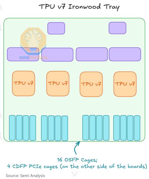
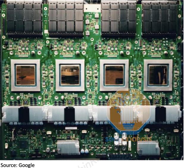
The meaning of the 6 ports should be viewed in the overall context first. Google arranges TPUs into a 3D grid, and the 6 ports are connected to 6 neighbors: up, down, left, right, front, and back (i.e. ±x, ±y, ±z), which is the 3D torus (figure below).
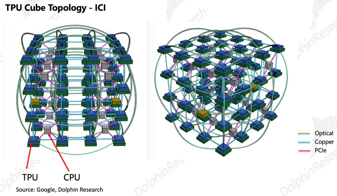
Back to the tray, you can see that the 4 TPUs in the tray are arranged in a row, but they are not interconnected in pairs. 4 of the 6 ports are reserved for neighbors on other trays, leaving only 2 ports in the board, so each TPU can only connect to 2 chips on the same board. Where the 4 ports out of the board are connected is the cross-tray topology in the next section.
2) Tray-Tray Scale-Up: Direct connection topology provides connectivity
The biggest difference from NVIDIA and AMD's solutions also lies in the Scale-up between trays: Google does not set switching chips, and TPUs are directly connected in a 3D topology.
16 trays form a Cube (i.e. rack) with a total of 64 TPUs, and the chips are connected into a 4×4×4 3D topology. Each chip is regarded as a 6-sided cuboid, and cables are pulled in six directions to directly connect with adjacent chips.
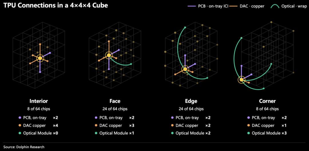
Looking at the topology in the figure below, you can see that some TPUs are connected not only by copper cables, but also by optical cables. What's the matter with that?
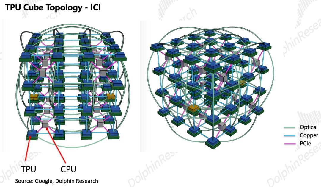
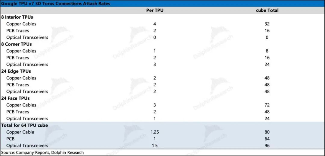
Whether to use copper or optical transmission depends on the position of the TPU in the domain. Inside a single Cube composed of 64 chips, the innermost 8 TPUs can be fully connected to all 6 adjacent TPUs through Copper (DAC+PCB).
Taking this 64-chip cube as a single Cube individual, since some sides of the TPUs on the edge have no adjacent TPUs, they are optically connected to the TPUs on the opposite side of the cube (see the green line). The TPUs on each outer edge are connected end to end, and the connection is converted into optical signals through the optical module and sent to the OCS switch. We have sorted out the corresponding connection devices and parameters of TPUs located at different positions (inside, surface, edge, corner) of the Cube, as shown below.
Using optical transmission directly at the Scale-Up layer is Google's unique design. The entire Scale-Up process of Vera Rubin NVL72 and Helios uses copper: GPUs are connected to NVSwitch/Tomahawk through backplane copper cables, optical modules only appear on the NICs and switches of Scale-Out, and the GPU itself does not access optical signals.
Google's optical module is directly inserted into the OSFP cage on the front panel of the TPU tray. The optical path is TPU → optical module → optical fiber → OCS → optical fiber → optical module → TPU, without any electrical switching equipment in the middle.
3) Cube-Cube Scale-Up: What is OCS?
As mentioned above, the optical cable connections on the outer surface of the Cube are aggregated into the OCS switch. In fact, in Google's larger network scale, it is also responsible for combining multiple Cubes into a larger domain: Pod (e.g. 4 Cubes, 256 TPUs) up to Superpod (upper limit 144 Cubes, 9216 TPUs). This is Google's most distinctive network hardware:
a. OCS switches are only responsible for redirecting optical signals. The signal links on the outer surface of the Cube are connected to the OCS through the optical module, and the OCS determines whether the other end of each link is looped back to form a 64-chip torus or combined into a larger torus. OCS is only responsible for guiding light from one port to another.
b. How are optical signals switched? OCS contains two sets of 2D MEMS micromirror arrays. By tilting each mirror on two axes, the light beam from any input port is "guided" to any output port (see the figure below). The essential difference from EPS (Electronic Packet Switch, the solution of AMD & NVIDIA) is: EPS makes real-time forwarding decisions for each data packet, while OCS establishes a static optical path between ports.
For example, if port 1 was originally connected to port 2, and now port 1 needs to communicate with port 4, OCS must reconfigure the mirrors because OCS has no forwarding function; while the ports of traditional EPS are fully interconnected, no reconfiguration is required.
A vivid example is railway switches: there can be multiple tracks, but only one is used at the same time, and to change the track, you must toggle the switch (i.e. adjust the mirror angle).
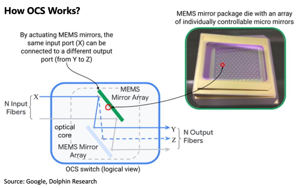
Therefore, it can also be said that Google's routing paths are pre-configured by software, because it is almost impossible to spend several seconds reconfiguring in low-latency workloads with synchronous parallelism.
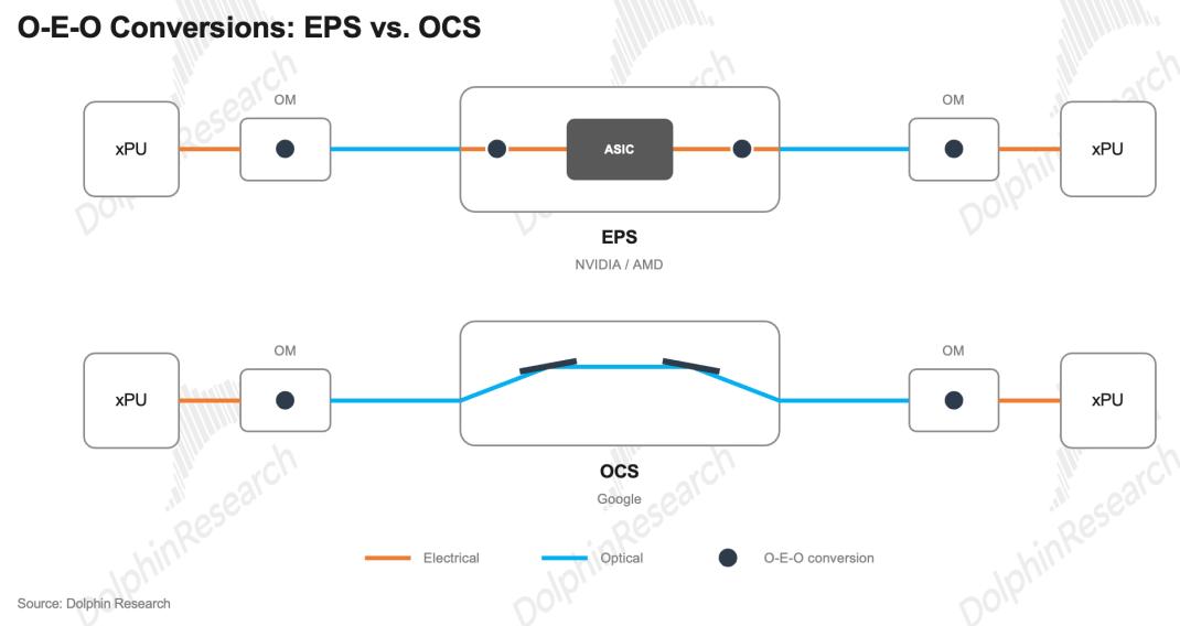
c. There is no O (Optical)-E (Electrical)-O (Optical) conversion process in the OCS switch. We know that in conventional EPS, the path of signals for communication outside the cabinet is: the signal emitted by the chip is an electrical signal, which is first converted into light (E→O) by the local optical module, and then transmitted to the switch through optical fiber.
The switch only recognizes electrical signals, the inlet converts light back to electricity (O→E), the switching chip decides which port to forward to, and the outlet converts electricity back to light (E→O); after passing through the optical fiber to the opposite cabinet, the optical module converts light back to electricity (O→E) and sends it into the chip.
What OCS saves is the two photoelectric conversions inside the switch. It is the only "switching" device in this network, but it does not need to bear the power consumption and cost of switching ASICs. The schematic diagram is as follows:
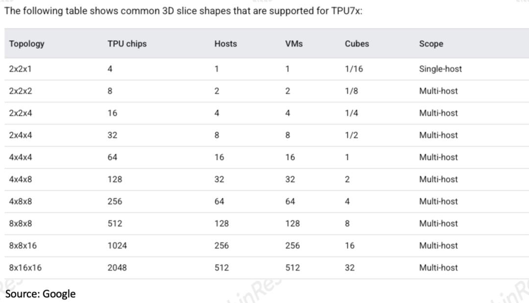
d. Flexible topology scale. In actual implementation, Google may not expand with the standard Cube (64 TPUs). Google can configure TPUs into common slice scales ranging from 4 to 2048, which is the flexibility provided by the pre-configuration of OCS switches.
4) Superpod-Superpod Scale-Out: Ambition of OCS to replace the Spine layer