Changxin Technology IPO: A Review of China's 36-Year Arduous Journey in the Memory Industry
1. CXMT Successfully Goes Public
Another Chinese enterprise that has helped the country break through tech bottlenecks has been listed on the stock market.
Just recently, CXMT, the largest DRAM chip manufacturer in China and the fourth largest worldwide, made its debut on the Shanghai Sci-Tech Innovation Board. Its opening price reached 49.5 yuan per share, surging 471.59% above the issue price, with a market cap exceeding 3.3 trillion yuan, making it the most valuable company on the A-share market.
The chips we commonly use fall into two main categories: logic chips and memory chips. CPUs and GPUs belong to logic chips; while the RAM in mobile phones and the memory sticks in computers are DRAM, or Dynamic Random Access Memory, a type of memory chip.
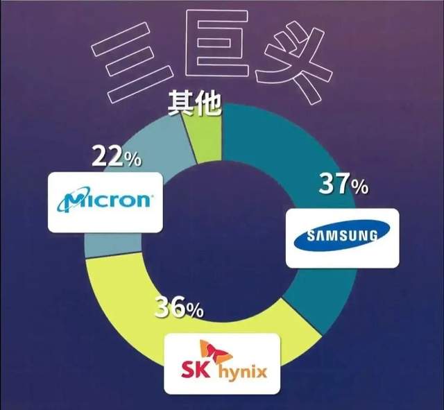
As the most mainstream memory chip, DRAM has long been a fiercely contested battlefield. After several industry cycles, the market was eventually monopolized by three giants: Samsung, SK Hynix, and Micron, which together hold over 90% of the global market share. However, CXMT has successfully broken through this monopoly. According to DRAM sales statistics for the fourth quarter of 2025, CXMT's global market share reached 7.67%, ranking fourth. (Source: Omdia)
As a leading domestic enterprise, CXMT already enjoyed a valuation premium, and with the superimposed price hike cycle of memory chips, investors were already calling for a trillion-yuan valuation for CXMT even before its IPO. Related concept stocks such as GigaDevice, Shangfeng Cement, and Hefei Urban Construction Development had already risen in advance.
Yet behind today's capital carnival lies China's arduous 36-year journey of memory industry development.
I previously explained why memory chip prices rise and what impacts this brings. Today, taking CXMT as a case study, I will walk you through the full development history of China's memory chip industry.
2. Obsolete Upon Completion: Huajing's 1.5 Billion Yuan Loss
In 1990, the State Planning Commission and the Ministry of Electronics Industry launched the "908 Project," allocating a total budget of 2 billion yuan to vigorously develop domestic chips.
Of this funding, 1.5 billion yuan was granted to Wuxi Huajing, the "greatest hope of the whole village" at the time, to build a large wafer fab with a monthly production capacity of 12,000 wafers. Huajing was a consortium composed of entities including the Yongchuan 24th Research Institute and Jiangnan Radio Component Factory, which undertook a large number of technology introduction projects in the 1980s.
In 1993, Huajing produced China's first 256Kb DRAM with a 2.5µm process node, marking a promising start. However, this was only a sample; Huajing did not achieve mass production of DRAM until 1997.
By that time, South Korea's chip technology had already become the world's leading force. Huajing's products used a 2.5µm process and 256kb capacity, while South Korea's chips adopted a 0.18µm process and 1Gb capacity — a gap of several generations, leaving Huajing "obsolete upon completion."
Coupled with the Asian financial crisis that shrank market demand, Huajing abandoned independent R&D in 1998 and transformed into a chip foundry. This marked the first time a Chinese enterprise voluntarily gave up its pursuit in the DRAM field.
3. Joint Venture with NEC: Huahai's Critical Setback
After Huajing exited the stage, Huahong took over the baton.
Shanghai Huahong was a key project under the "909 Project." Adopting the "market for technology" strategy, Huahong formed a joint venture with Japan's established tech giant NEC in 1997 to enter the DRAM sector. In September 1999, Huahong began mass production of 64M DRAM using a 0.35µm process, a technological level far exceeding that of Huajing two years prior. The following year, Huahong achieved 3 billion yuan in sales.
After that, progress came to a halt. The 2000 Nasdaq crash caused Huahong NEC to suffer a huge loss of 1.348 billion yuan.
The Nasdaq crash was only an external factor; the core problem remained technological backwardness. The 0.35µm process and 64M capacity seemed advanced, but Samsung had already achieved mass production of such products back in 1992 — a full seven years earlier than Huahong.
In fact, by the late 1990s, Japan's chip technology had already fallen behind South Korea. Choosing to source technology from Japanese companies predetermined that it would not be cutting-edge. Since South Korea refused technological cooperation, China had no choice but to settle for second-best options.
The Nasdaq crash did not defeat Huahong, but it shattered NEC. In 2001, this faltering tech veteran announced its withdrawal from the DRAM market. This left Huahong in a dire situation: although NEC's technology was outdated, it was still a mid-tier performer that could share its "homework" with Huahong. Now that the mid-tier student had dropped out, and top-tier players refused to collaborate, what could they do?
In 2003, Huahong also exited the DRAM sector and transformed into a chip foundry, joining its former peer Huajing.
4. The DRAM Industry Enters the Era of Three Global Giants
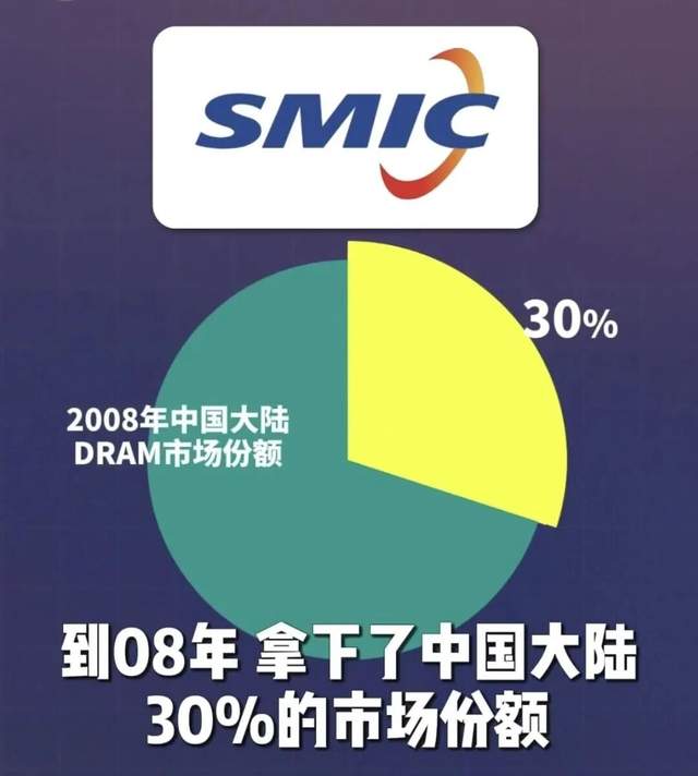
Later, SMIC took over the relay, partnering with Europe's top chip firm Infineon in 2006 to produce DRAM using an 80nm process. By 2008, SMIC had captured 30% of the mainland China market share. However, the subsequent financial crisis caused DRAM prices to plummet. As a peripheral business for SMIC, DRAM soon became a financial drag. Shortly after, SMIC abandoned its DRAM business and focused exclusively on chip foundry services.
SMIC was not an isolated case. The 2008 financial crisis profoundly reshaped the global DRAM landscape. Afterwards, Europe's Qimonda went bankrupt, Japan's Elpida was acquired by Micron, and the DRAM industry entered the "three giants" era dominated by Samsung, SK Hynix, and Micron.
5. Beginner's Guide: DRAM Requires the IDM Model
At this point, you may wonder: why did all companies that previously worked on DRAM switch to foundry services after exiting the DRAM market? What is the relationship between DRAM and foundry operations?
As explained earlier, DRAM falls under memory chips, while CPUs and GPUs are logic chips.
Different types of chips have vastly different production models.
Memory chips typically adopt the IDM (Integrated Device Manufacture) vertical integration model, meaning companies handle everything from designing, manufacturing, to selling their products — even producing their own packaging materials. Giants like Samsung, SK Hynix, and Micron all operate under the IDM model.
Logic chips usually adopt the Fabless (fabless) model, where manufacturing is outsourced to foundries, and the company only focuses on designing and selling chips. NVIDIA, Qualcomm, AMD, and HiSilicon all belong to this category, while TSMC and SMIC are the foundries responsible for their chip manufacturing.
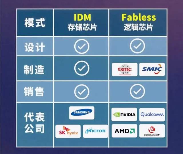
The core difference between the two models lies in whether the company owns its own "oven" — that is, a wafer fab.
Virtually all memory chip manufacturers have their own wafer fabs. After abandoning their memory business, these existing fabs can take on manufacturing orders from other companies, which is why they transition to foundry services.
Curious readers may ask: why do memory chip companies own wafer fabs, while logic chip firms do not?
The decision to build a wafer fab or not is a trade-off between profit and speed.
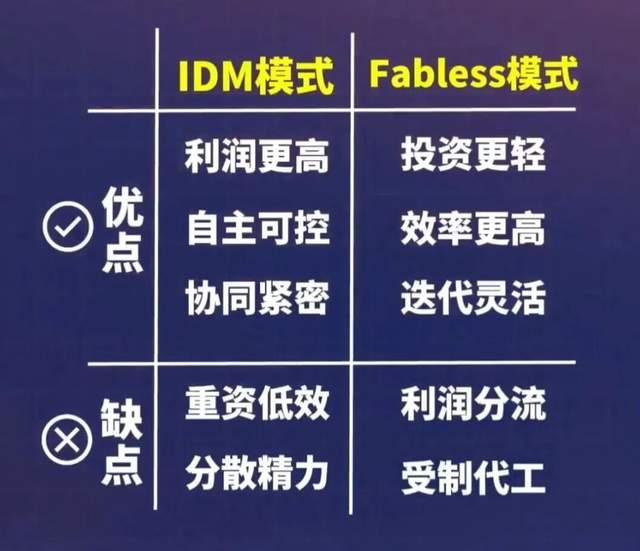
The benefits of self-designing and self-manufacturing chips are obvious: no profit margin is lost to suppliers, profits are higher, there is no risk of being restricted by external bottlenecks, the full process can be independently controlled, and the coordination between design and manufacturing is more seamless. However, the downsides are heavy capital investment and low efficiency. A large wafer fab often costs tens of billions of dollars to build, a sum that very few companies in the world can afford. Moreover, handling everything in-house inevitably disperses management focus. If technological iteration speeds up, it becomes difficult to keep pace with the industry. If product updates also accelerate, the situation becomes even worse: production lines built with massive investment will soon become obsolete, causing huge asset impairment losses.
In contrast, the Fabless model has the advantages of low investment and high efficiency, making it suitable for products with rapid iteration cycles. Its disadvantages include sharing part of the profits with foundries and the risk of being constrained by foundry partners.
Now that we have clarified the pros and cons of the two models, let's examine the two categories of chips.
Logic chips such as CPUs and GPUs, as core performance components, face extremely fierce technological competition and iterate on an almost annual basis. Think about Apple, Huawei, and Xiaomi — all their flagship products are updated on a yearly cycle. In comparison, memory chips are far more stable, with a single generation of products remaining viable for at least three to five years.
Therefore, memory chips are more suitable for the IDM model, while logic chips are a better fit for the Fabless model. In fact, before TSMC was founded, the entire industry operated under the IDM model, with no companies specializing in pure foundry services. But Morris Chang predicted that logic chips would iterate rapidly in the future, and the value of chip design would grow larger. Thus, he founded TSMC to focus on providing manufacturing services for chip design firms, rewriting the entire industry landscape.
AMD is another illustrative case. Founded in 1969, AMD initially operated under the IDM model. In the early 1990s, when TSMC was just emerging, a reporter asked AMD's founder Jerry Sanders for his opinion, and he famously said: "Real men have fabs."
However, entering the 21st century, AMD was suppressed by Intel for years, and suffered huge losses after acquiring graphics card maker ATI. In 2008, AMD sold off its wafer fabs and transformed into a pure chip design company, which unexpectedly allowed it to turn its business around.
Of course, this conclusion is not absolute. Domestic companies like GigaDevice and Jiangbo Long also focus on memory chips, but they only engage in secondary design and packaging without owning their own wafer fabs. Meanwhile, Texas Instruments, which adheres to the IDM model, also operates its own logic chip business. However, none of these companies can be regarded as top-tier industry leaders.
6. The "Tough Guy" Boss Zhu Makes China's DRAM Dream Come True
End of the popular science section, let's return to the development history of China's DRAM industry.
After Huajing, Huahong, and SMIC successively exited the DRAM sector, the Chinese government did not stop supporting the DRAM industry.
Especially after 2010, with the popularization of PCs and smartphones, the DRAM market expanded rapidly, and the importance of independent and controllable DRAM supply increased significantly.
On June 24, 2014, the State Council issued the "National Integrated Circuit Industry Development Promotion Outline," elevating the chip industry to a national strategic level. Three months later, the National Integrated Circuit Industry Investment Fund, dedicated to investing in the chip sector, was established. The first phase raised 138.7 billion yuan, and the second phase raised 204.15 billion yuan — a level of support far exceeding that of the 908 and 909 projects.
In 2016, Zhu Yiming, the founder of GigaDevice, embarked on his second entrepreneurial venture. With the support of the Hefei municipal government, he founded CXMT.
Boss Zhu is a true "hardcore tough guy." He was admitted to the Department of Physics at Tsinghua University at the age of 17, completed his bachelor's and master's degrees consecutively, then went to the United States for further studies. After graduation, he worked at a chip design company in Silicon Valley (Monolithic System Technologies).
In 2005, 32-year-old Zhu Yiming returned to China to start his business, founding GigaDevice to engage in DRAM and MCU (Microcontroller) design.
In 2016, GigaDevice went public, but Boss Zhu turned his attention to building CXMT.
He clearly understood that to become a top-tier DRAM enterprise, one must be a "real man" and own its own wafer fab.
With the capabilities of GigaDevice alone, this goal was impossible to achieve — cooperation with state-owned capital was a must. At that time, Hefei was suffering from the "chip shortage pain" experienced by its display industry, and the two sides reached an immediate consensus.
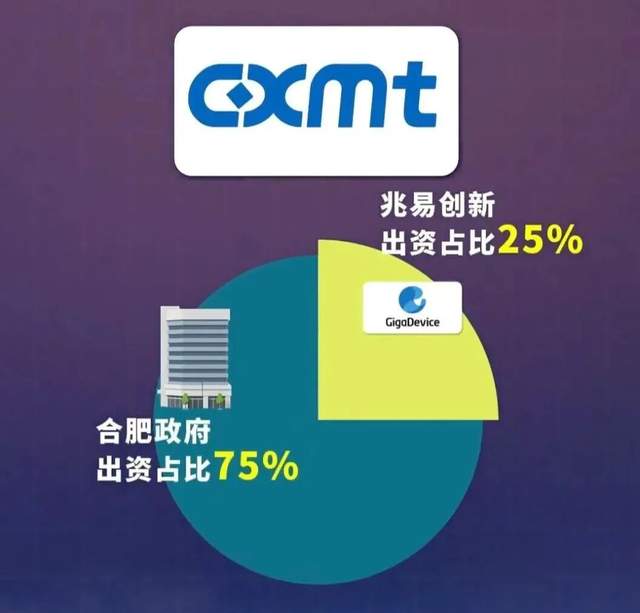
On June 13, 2016, Hefei Changxin was established. The first phase of construction invested 18 billion yuan, of which GigaDevice contributed 1/4, and the remaining 3/4 was fully funded by the Hefei municipal government.
Boss Zhu not only invested capital but also dedicated enormous effort. On July 16, 2018, CXMT's 12-inch DRAM wafer production line — the largest single production line of its kind in China — was officially put into operation. On the same day, Boss Zhu announced his resignation as General Manager of GigaDevice, retaining only the position of Chairman, and took up the post of CEO at CXMT. He even issued a military order that he would not receive a single penny of salary or bonus before CXMT turned profitable. The prospectus shows that Boss Zhu indeed never drew any salary during that period.
However, in the fourth quarter of 2025, CXMT turned losses into profits, and it is expected to achieve huge earnings this year. It remains to be seen whether the company will pay Boss Zhu his well-deserved salary.