Domestic chips are gearing up for a three-stage leapfrog development.
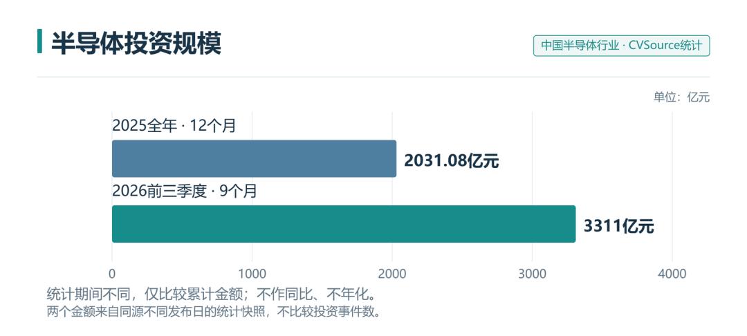
In the first three quarters of this year, the investment received by China's domestic semiconductor industry has exceeded the total amount of the whole of last year. According to statistics from CVSource by ChinaVenture, the total investment amounted to 3.311 trillion yuan, with 1,475 investment events. Entering November, new financing of computing chip enterprises is still being disclosed.
Products that capital is willing to wait for have taken on a different look. Some chips have been delivered to customers' computer rooms, and new funds are used to prepare for the next generation; some have just got sample chips back from the factory, and still need to go through testing and complete machine adaptation. Financing news puts these companies on the same list, but customer procurement will follow a completely different sequence.
The three-leap forward that domestic chips are preparing for is hidden in this gap: investment is first converted into usable products, then forms a supply system that supports continuous iteration, and finally changes the way customers allocate orders. At present, different enterprises are at different development stages. While a batch of new products are still striving for their first large-scale market, CXMT and YMTC have pushed the competition to process upgrading and product portfolio optimization. What is more noteworthy is that NVIDIA's growing influence has different impacts on domestic accelerator and storage manufacturers: the former faces higher replacement thresholds, while the latter may still tap into new demand from the expanding computing system.
Nearly 100,000 Chips Sold, The Next Generation Still Needs to Pass New Validation
In early November, Lingchuan Technology completed a 1 billion-yuan Series B financing. According to information disclosed by investor Qiming Venture Partners, its SL200 intelligent video chip has accumulated nearly 100,000 units sold, with customers including Kuaishou, Alibaba Cloud and Baidu Cloud. The next-generation chip for AI video production was taped out in April this year and samples were returned recently, with the mass shipment target set for 2027.
For the same company, there is still a full round of product development between the chips that have been sold and the new business to be won. Traditional video processing and AI video generation consume different computing resources. Optimizing video coding efficiency does not automatically fulfill the operations required by generative models. To this end, Lingchuan adopts a 3D stacking solution, develops a unified computing platform, and adapts to models including Tongyi Wanxiang and Hunyuan Video. The customer relationships accumulated by old products can help new products access real business scenarios; the new generation of chips still needs to re-prove their performance and cost advantages in these scenarios.
After receiving sample chips, the chips still need to go through testing, software adaptation and mass production preparation before they can become deployable products for customers. The new funds will cover the pre-delivery investment, and also enable the enterprise to continue developing the next generation while maintaining existing businesses. Storage manufacturers demonstrate this kind of continuous competition more clearly: products need to be upgraded, manufacturing processes also need to advance, and faster interfaces and larger capacities must ultimately land at costs that customers can afford.
Domestic Storage Starts to Compete for Flagship Phone and Server Orders
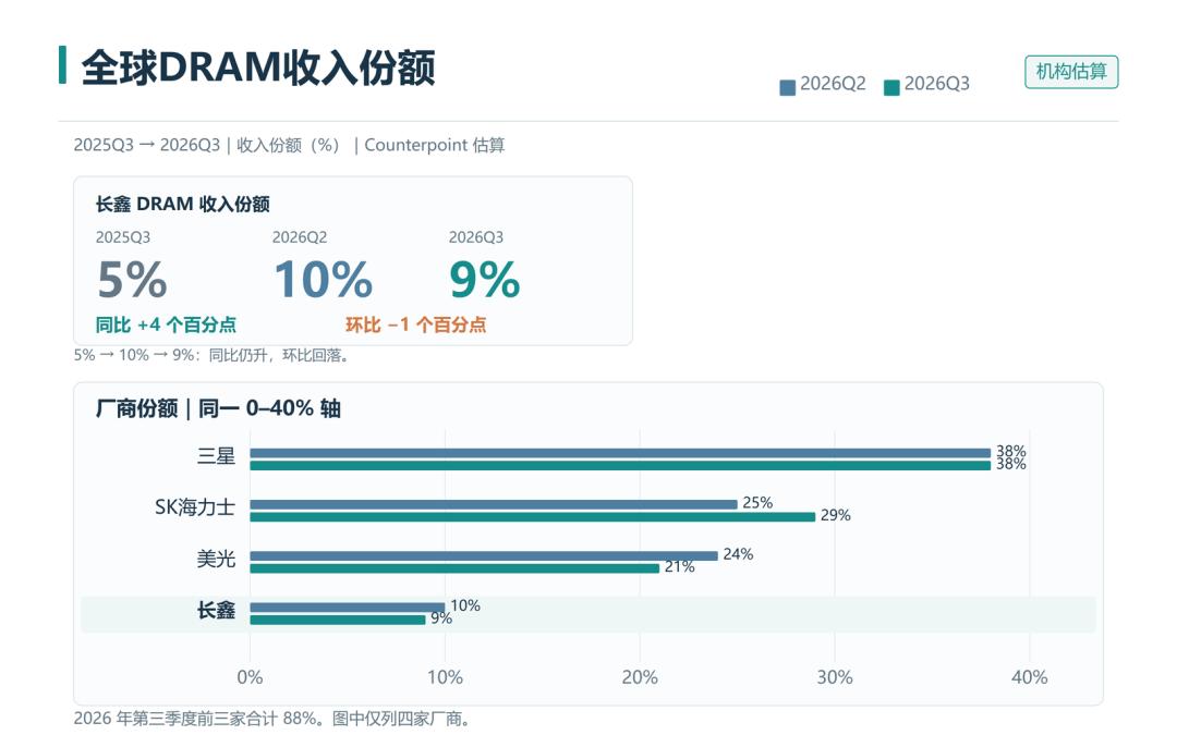
The changes of CXMT have already been reflected in the revenue distribution of the global storage market. Data released by Counterpoint on November 5 shows that in the third quarter of this year, CXMT's DRAM revenue share was 9%, down 1 percentage point from 10% in the second quarter, but still 4 percentage points higher than 5% in the third quarter of last year. Samsung, SK Hynix and Micron together account for 88%. The three major manufacturers continue to dominate the market, but customer procurement has already accommodated a new participant that holds nearly one-tenth of the total market revenue.
In September this year, CXMT announced the mass production of its fifth-generation DRAM technology platform G5, and simultaneously launched the LPDDR5X product with a single-die capacity of 24Gb. The miniaturization of memory chips ultimately aims to maximize the storage capacity that a single wafer can carry. Converted based on the unified 8Gb die benchmark, CXMT disclosed that the number of dies per wafer of G5 is at least 50% higher than that of G4. With the same wafer area, more storage capacity can be accommodated, so the investment in factories and equipment can be allocated to more products. The actual cost also depends on processing steps, yield and production line utilization, and the increase in density opens up large space for cost reduction.
This also explains why process iteration needs to be carried out continuously. Mobile phone manufacturers have to rearrange memory capacity, bandwidth and total machine cost every year. Entering the supply chain in the previous generation is only the starting point for the next round of competition. CXMT disclosed in the same September that its LPDDR6 has been launched on the Xiaomi 18 Fold, providing 16GB packaged capacity with a transmission rate of 10667Mbps when paired with the processor. It has begun to participate in the terminal implementation of the new-generation memory standard, so product competition has advanced from completing existing specifications to keeping up with the development rhythm of flagship mobile phones.
Peer competitors in the same generation are also promoting this progress. Samsung's publicly announced 16GB LPDDR6 has completed sample delivery and verification on Qualcomm's new-generation Snapdragon platform, with a maximum I/O rate of 10.7Gbps. The two products are in similar ranges of capacity and transmission rate: CXMT disclosed its terminal commercialization progress, while Samsung disclosed its platform verification progress, corresponding to different cooperation stages respectively. CXMT has entered the competition of same-generation products; power consumption, mass production cost and long-term reliability cannot be ranked simply by these two specifications.
G5 and LPDDR6 correspond to the manufacturing platform and product standard respectively. The former improves the storage capacity provided per wafer, while the latter gives mobile phone manufacturers an extra choice when developing new-generation flagship devices. Keeping up with industry standards and entering terminal products enables domestic memory manufacturers to have specific products that can participate in the design of new-generation flagship devices; continuous improvement of manufacturing cost determines how many models they can cover and how large-scale procurement they can undertake.
YMTC faces another type of storage demand. Photos stored in mobile phones and training data on servers need to be retained even after power off. NAND flash undertakes this type of work in mobile phones and servers equipped with SSDs. It also needs to improve storage density, but after entering the data center, what customers usually buy is a SSD that can work continuously, so product capabilities beyond the flash particles themselves become equally important.
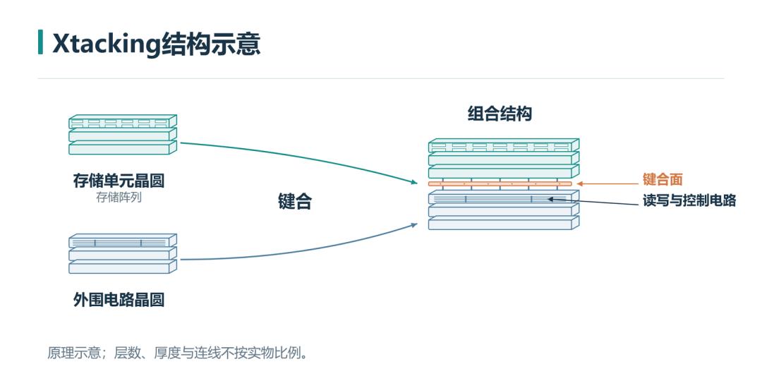
YMTC's Xtacking architecture manufactures storage units and peripheral circuits responsible for data reading, writing and control separately before connecting them together. In this way, the processes of the two parts can be arranged independently: the storage units can pursue higher density, and the peripheral circuits can improve data transmission capability. The company's product roadmap shows that the fifth-generation TLC flash was mass-produced in 2024, and the fifth-generation QLC was launched in 2025, with technology continuing to iterate along the same route. Previously, TechInsights confirmed the two-wafer hybrid bonding structure of Xtacking 4.0 in the ZhiTai TiPlus7100 Black Myth Edition SSD, indicating that this manufacturing route has been applied to sold finished products.
The difference between TLC and QLC can be understood from the perspective of capacity: one storage unit stores 3 bits and 4 bits respectively, so QLC can hold more data with the same number of units. YMTC's PE501 enterprise-level SSD adopts QLC, with a maximum capacity of 122.88TB. The same amount of data can occupy fewer drive bays, which has practical value for computer rooms. International manufacturers have already laid out products in this capacity range: Solidigm released the 122.88TB D5-P5336 in November 2024, and had already delivered samples to customers at that time. YMTC has entered the corresponding product segment, and competition beyond capacity has subsequently unfolded.
For databases that are frequently updated and storage that mainly undertakes data reading tasks, the requirements for capacity and write endurance are different. YMTC simultaneously provides the TLC-based PE522, and divides it into configurations that focus on read scenarios and mixed read-write scenarios. This product portfolio allows it to arrange capacity, endurance and price for different businesses, instead of using one maximum-capacity product to cover all customers.
Entering the server supply chain also requires system verification. In the NVMe list of the Interoperability Lab at the University of New Hampshire in the United States, PE501 with the specified firmware version was registered in January this year, and PE501N was registered in October. This list records interoperability and conformance tests, indicating that the product has reached the stage of joint verification with external systems. For enterprise-level SSD manufacturers, competition also includes how to reduce the workload of customers in verifying new products. When Solidigm released its 122.88TB product, it specially introduced that its high-capacity products from 7TB to 122TB share the same controller, which facilitates customer verification. Launching more capacity specifications around existing software and hardware can make one product introduction cover a wider range of procurement demands.
Therefore, YMTC's expansion to enterprise-level SSDs is also changing the division of labor between itself and customers. When selling flash particles, the full-drive design can be completed by downstream customers; when providing enterprise-level SSDs, the controller, firmware, data protection and subsequent services need to be integrated into the product. Counterpoint pointed out in its October analysis that YMTC benefited from both rising prices and domestic sales growth, and it had not fully obtained the premium of the enterprise-level SSD market before. Expanding supply on the manufacturing end and establishing product position among high-value customers have become two tasks that need to be promoted simultaneously.
Changes have taken place in global revenue distribution. Counterpoint estimates that YMTC's revenue share in the NAND market rose from 11% in the second quarter of 2025 to 14% in the same period this year. This growth occurred during the storage price increase cycle. The same institution estimates that NAND prices rose 55% quarter-on-quarter in the second quarter of this year. Price increase can raise the total revenue of the entire market, and the increase in market share indicates that YMTC has captured a larger part of the incremental revenue.
Purchasing AI Chips Requires Calculating the Cost of the Entire System
While domestic chips continue to receive investment, competitors' products are also advancing. On October 27, NVIDIA and Oracle announced that Vera Rubin NVL72 and Vera CPU are officially available on the OCI cloud platform. The next-generation platform that was only shown at the press conference at the beginning of the year has now entered the product catalog of cloud services.
The scope of competition demonstrated by Rubin goes far beyond a single GPU. One NVL72 rack connects 72 GPUs through NVLink, and the system also requires CPU, network, data processor and software to work in coordination. When users run models, if the computing units cannot get data in time, or the communication between multiple GPUs is not smooth, the nominal computing power cannot be fully utilized. NVIDIA promotes all these links together, so the objects of comparison for customers have expanded to the entire system.
Domestic accelerators are also accumulating capabilities in these specific practices. In January this year, Baidu publicly shared its practice of deploying DeepSeek R1 on the Tianchi super node: each super node connects 32 Kunlunxin XPUs. Based on the SGLang inference framework, the team deployed input processing and answer generation separately, then adjusted model distribution, video memory occupation and communication scheduling. To make room for longer context, different experts of the model are distributed to more cards, and the weight carried by each single card is reduced accordingly. System optimization has been implemented to how the model runs, rather than staying at the level of chip parameters.
These practices also show that the price of a single card is only part of the procurement cost. The precision at which the same model runs, how long it takes to give answers, and how many requests it can serve at the same time will all affect the number of servers that need to be deployed. For customers who already have a large number of businesses running on a certain platform, the time consumed for migrating models and maintaining software also needs to be included in the input of switching solutions.
However, global technology upgrading and Chinese customers' access to products are two coexisting facts. NVIDIA's quarterly filing as of July 26 this year shows that only part of the H200s licensed to supply Chinese customers have been shipped, and these shipments account for less than 1% of its data center revenue in the quarter. The opportunities for domestic manufacturers still include the demand for stable supply. It can help enterprises enter customers' verification and procurement processes, and leave time for software adaptation and customer service accumulation.
If NVIDIA's actual supply for China expands and its price is competitive enough, products that rely on supply gaps will face stricter comparison. Domestic accelerators need to accumulate advantages in the most frequent tasks run by customers, rather than only providing alternatives when procurement is restricted. Lingchuan's shift to video generation is an attempt to concentrate hardware and software investment on specific scenarios. Dedicated design can arrange data flow around relatively stable computing characteristics, but model changes will also affect the original advantages. Behind the 2027 shipment target, the core goal is to convert today's customer access into the usage reason for the new generation of products.
NVIDIA Enables Flash Memory to Share AI Inference Cache Workloads
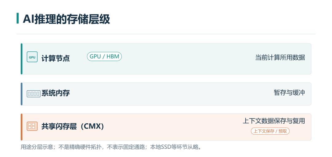
The enhancement of NVIDIA's platform is also expanding workloads beyond computing. Its newly announced CMX context storage platform is specifically designed to process a type of data in AI inference: KV cache generated when the model processes long conversations and continuous tasks. Retaining these intermediate results allows subsequent calculations to reuse existing work, reducing the overhead of reprocessing historical content. For answers being generated, latency-sensitive data needs to be close to the GPU and placed in the high-bandwidth memory HBM; system memory is responsible for temporary storage and buffering; local SSD and shared storage undertake larger capacity tasks.
CMX adds a shared context storage layer based on flash memory between these tiers, allowing a group of computing nodes to access the cache, and send data back to GPU or system memory in advance when necessary. Long conversations, more concurrency and continuously running agents increase the amount of data that needs to be saved, moved and reused. The system retains high-speed space close to the GPU on one hand, and uses larger-capacity storage to carry other data on the other hand, so as to balance performance and cost.
This leaves different opportunities for storage manufacturers compared with accelerators. Domestic accelerators strive for the transfer of computing tasks, which requires customers to rearrange models, software and servers; storage manufacturers can strive for new procurement when the computing system continues to expand, without waiting for a certain domestic GPU to become the market leader. NAND flash, DDR & LPDDR, and HBM serve different positions, and which part of the order to obtain depends on the specific products and customer verification. CMX demonstrates how new demand is formed. CXMT's progress in the mobile phone memory market and YMTC's expansion to enterprise-level SSDs reflect the scope that the existing products of the two manufacturers can participate in.
The rising revenue share of CXMT and YMTC has pushed domestic supply from the stage of "whether the product exists" to the stage of "how to allocate orders". For customers, one more supplier that can keep up with product iteration means one more option to arrange prices and supply risks; for chip enterprises, participating in the development of new-generation terminals and servers can turn manufacturing and software investment into specific demand. The new funds pouring in now are enabling more enterprises to get the opportunity to participate in this round of selection. Only when customers continue to adopt domestic chips in next-generation products can the breakthrough supported by one round of financing be turned into a sustainable industrial position.