Micron DRAM and NAND, latest roadmap
Last month, Micron Technology unveiled its DRAM and NAND flash development roadmap for the coming years, revealing its plans to adopt wafer bonding technology, new materials to shrink NAND flash cell sizes, and High-NA EUV lithography, and detailed its progress toward 3D DRAM.
Perhaps the most notable part of Micron's current plan is that as AI developers' demand for memory and storage solutions optimized for their unique processor architectures and specific workloads grows, the company plans to expand its custom DRAM and NAND product portfolio.
"DRAM is now approaching atomic-level limits: while we are confident in the next few planar nodes, we are very focused on ensuring that 3D DRAM is launched at the optimal time in terms of cost and performance," said Scott DeBoer, President, Chief Technology and Products Officer of Micron Technology, at a company event earlier this month. "For 3D NAND, our real focus is on leveraging new materials to increase the density of cell structures, and continuing to work on future XYZ scaling."
DRAM: 4F² Cell Phased Out
Surprisingly, Micron has decided to abandon the production of DRAM with 4F² memory cells, which is a very different approach from competitors such as CXMT, Samsung and SK Hynix. Micron says that no viable scaling path can be found with current technological development. Instead, Micron's roadmap for the coming years includes wafer bonding, High-NA EUV lithography, new materials, and eventually 3D DRAM. The company plans to start mass production of its next-generation 1δ memory in the second half of 2027, while the subsequent 1ε, ζÅ and ηÅ technologies are in different stages of R&D. At the same time, Micron is developing two generations of 3D DRAM, which are expected to eventually replace traditional planar memory.
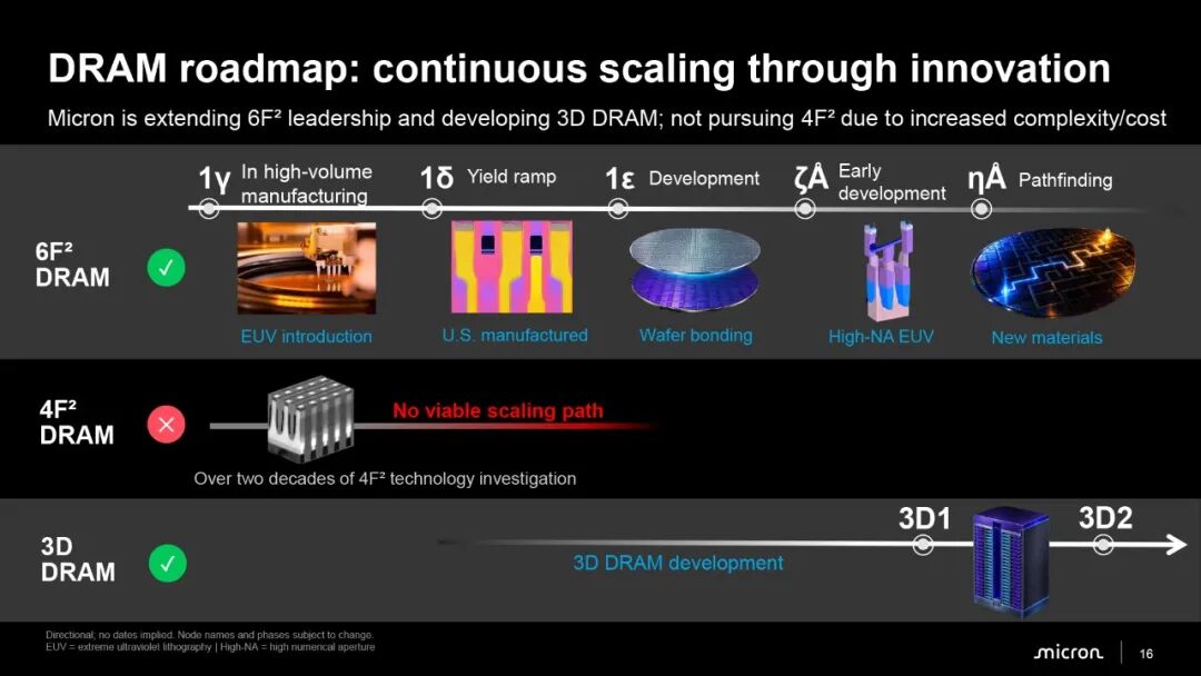
Micron's 1γ (1-gamma) DRAM process technology, which is currently in mass production, is the company's first DRAM node using EUV lithography. Previously, Micron had been using multi-patterning processes with DUV lithography and remained competitive with Samsung and SK Hynix, which relied on EUV lithography to manufacture critical layers.
Micron Technology's next-generation 1δ (1-delta) manufacturing process is currently in the yield ramp-up stage, and is scheduled to enter mass production in the second half of 2027. The company expects this technology to increase bit density by around 20% compared to the 1γ process, while advanced high-k metal gate (HKMG) CMOS, new materials, angstrom-level process control and equipment intelligence will improve performance, energy efficiency, and ultimately increase yield and reduce costs.
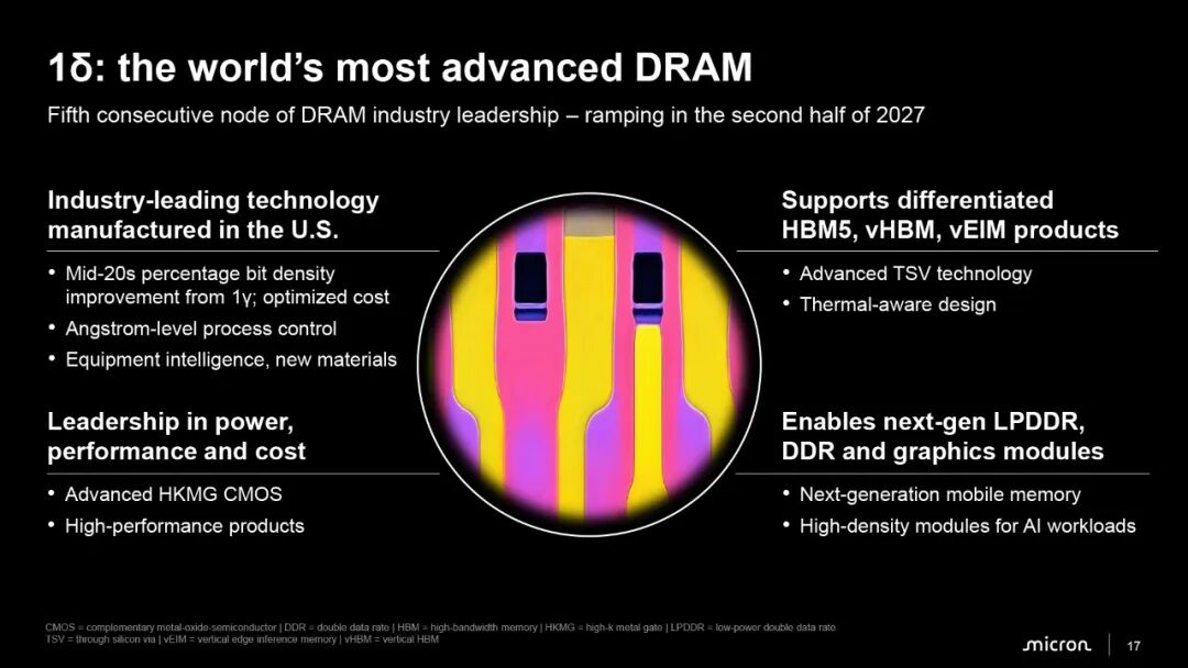
Micron plans to manufacture 1δ DRAM in the United States, and apply this technology to next-generation DDR, LPDDR, graphics memory, HBM5, vertical HBM (vHBM) and vertical Edge Inference Memory (vEIM) products. At the same time, to produce HBM5, vHBM5 and vEIM products, this process node will also support additional features such as Through-Silicon Vias (TSVs) to improve heat dissipation performance.
The subsequent 1ε (1-epsilon) process will adopt wafer bonding technology, enabling Micron to fabricate different structures on separate wafers and then bond them together. This approach can improve the flexibility of memory design and manufacturing, but Micron has not announced its specific implementation plan for wafer bonding, including which structures will be bonded, and what improvements this technology will bring in terms of density, performance and power consumption. This process is still under development, and no mass production schedule has been announced.
Micron's ζÅ (zeta-angstrom) production node is still in the early R&D stage, which will introduce High-NA EUV lithography into memory manufacturing to further reduce critical dimensions. The company has not disclosed the number of layers that require High-NA lithography, the expected density improvement, and when this technology will be put into mass production. However, it is obvious that this node will not be available until at least 2030, several years later than Samsung and SK Hynix's adoption of High-NA EUV technology in their DRAM fabs (planned for 2028).
The ηÅ (angstrom) process is the furthest generation in Micron's publicly disclosed planar DRAM roadmap, and is still in the exploration stage. After Micron introduces High-NA EUV lithography into its DRAM production flow, the company plans to try other scaling technologies. Although Micron mentioned new materials, it did not specify these materials, nor did it explain how they would affect device structures. These new materials may include new types of photoresists, deposition precursors, dielectric materials or conductive materials, which will enable Micron to manufacture smaller transistors and capacitors, and ultimately increase DRAM cell density.
3D1 and 3D2:
The Transition to 3D DRAM is Coming
While conducting traditional DRAM R&D, Micron Technology is also developing two generations of 3D DRAM, currently called 3D1 and 3D2. Unlike planar DRAM, which mainly relies on smaller memory cells to increase bit density, 3D DRAM uses the vertical dimension to accommodate more memory cells in a given area. Micron plans to launch this technology when the manufacturing cost and performance of 3D DRAM are comparable to those of traditional DRAM. The company has not announced its architecture, layer count or target density.
In short, Micron's roadmap focuses on continuing to develop DRAM based on 6F² cells, which is different from the plans of CXMT, Samsung and SK Hynix.
In fact, although Micron has outlined its future memory architecture up to 2030, its DRAM manufacturing roadmap only provides a clear production window for the 1δ process, which is scheduled to enter mass production in the second half of 2027. The company has not disclosed the production dates for subsequent planar DRAM nodes or any generation of 3D DRAM.
Customized HBM and Vertical Memory Architecture
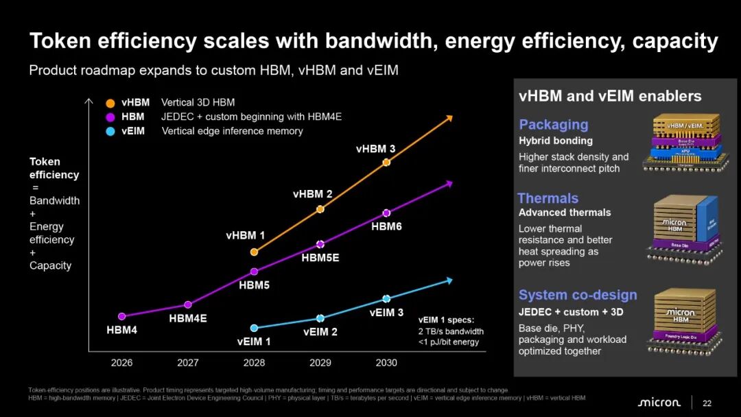
In addition to traditional DRAM, Micron plans to apply its future manufacturing technologies to HBM4E, HBM5, HBM5E, and new vertical integrated memory architectures. First, the company will offer standard HBM4E and customized HBM products, followed by customized HBM5E, vHBM and vEIM (vertical Edge Inference Memory). All of these will mark the resurgence of customized memory products in mass-produced offerings.
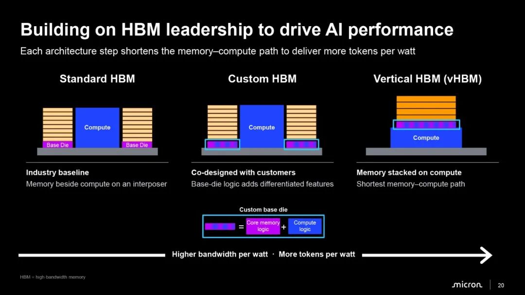
Customized HBM4E (cHBM4E) will enable Micron's customers to reduce the memory I/O width, and/or integrate additional logic into the memory's base die, freeing up valuable die space for computing, and optimizing performance and power consumption for specific AI accelerators. Scott DeBoer, President, Chief Technology and Products Officer of Micron, said that some of these features were originally located on the ASIC die itself, so moving them closer to the memory should improve overall system efficiency.
"When we co-design the base die, it is often the case that some logic elements that were supposed to be placed in the GPU circuit are offloaded to the base die in order to bring the base die closer to the memory. At the development stage of vertical HBM, it is still realistic to move more reasonable functions to the base die," DeBoer said.
To support these features, Micron plans to use advanced foundry process technologies on the base dies of standard and customized HBM products, but has not disclosed specific process nodes. For customized designs, the company will select the most cost-effective process that meets customer requirements. For example, Micron expects HBM4E to require more advanced CMOS technology to meet its performance and power consumption targets.
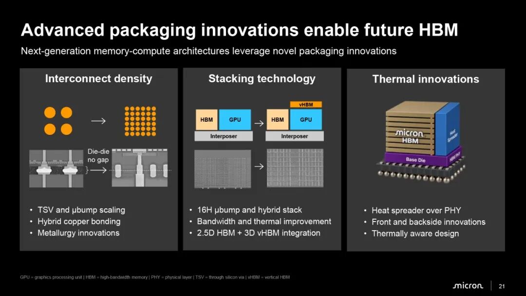
In the future, Micron plans to launch vertical HBM (vHBM) technology, which stacks memory directly on top of ASICs and CPUs, instead of placing them side by side through an interposer like traditional HBM. This architecture is expected to significantly increase bandwidth, thanks to dense vertical connections (and significantly reduced latency brought by adjacent placement), but it also brings huge challenges related to power supply and heat dissipation. To address these challenges, Micron plans to use hybrid bonding technology to achieve advanced interconnections, and integrate heat sinks and thermal-aware designs. Notably, the company expects that traditional HBM and vHBM will coexist in some designs, where vHBM provides maximum bandwidth while traditional HBM meets capacity requirements.
Another technology under development is vertical Edge Inference Memory (vEIM), which shares many packaging and integration technologies with HBM, but its target applications focus more on energy efficiency rather than maximum bandwidth. Micron's first-generation vEIM aims to deliver 2TB/s bandwidth similar to HBM4, while keeping the energy consumption per bit of data transmission below 1 picojoule.
Both of these architectures require close cooperation with customers to optimize the memory, logic, packaging and thermal characteristics for specific applications, so Micron needs to work hand in hand with customers to ensure the success of vHBM and vEIM. Notably, Micron's customer-specific development work is not limited to HBM and EIM.
For example, the company is working with Meta to optimize the performance of LPDDR6 for data center applications, focusing mainly on reliability, maintainability and availability. Micron expects LPDDR6 to consume about 35% less power than LPDDR5, which is critical for high-density memory deployments. In addition, the company plans to work with major customers to develop DDR6 (whose bandwidth target is twice that of DDR5) to better understand and ultimately meet their needs.
When talking about customer collaboration, DeBoer emphasized that Micron now collaborates with customers from the very beginning of product definition, throughout co-design, development, verification and mass production. The executive said that this approach is very different from the company's previous customer collaboration model.
"In all our AI co-innovation projects, we are co-conceiving, co-designing, co-developing, co-verifying, and then delivering at scale," DeBoer said. "This opportunity is truly unique. It is very different from the way we interacted with customers three or four years ago."
Advanced CMOS: More than 10x Performance Improvement
In addition to shrinking DRAM cell sizes and developing vertical memory architectures, Micron Technology is also developing advanced CMOS technologies for peripheral circuits. The company's roadmap includes several generations of DRAM CMOS logic circuits with high-k metal gate transistors, as well as first-generation and second-generation 3D CMOS technologies.
Micron expects these technological advances to increase its CMOS logic performance by more than 10x between 2020 and 2030, which will help the company meet the growing bandwidth and power consumption demands of AI-oriented memory products.
3D NAND: From 400-Layer 3D NAND
to AI-Oriented NAND
While Micron's event focused mainly on the future of DRAM, the company also shared some details about its upcoming NAND innovations, including 400-layer 11th-generation 3D NAND, post-G11 3D NAND, and AI-oriented NAND memories that offer either high bandwidth or high IOPS.
Micron Technology's next-generation G11 (N170) 3D NAND technology represents a significant improvement over its current G9 (N160) process. The company plans to increase the number of active memory layers from 276 to over 400, introduce wafer-level bonding technology, and adopt industry-leading memory cell spacing.
These improvements are expected to double the bit density of G11 3D NAND compared to G9 3D NAND, and the bit density of 3D TLC devices may increase from 21 Gb/mm² to 42 Gb/mm², which will significantly reduce the manufacturing cost per bit once this technology reaches mature yields.
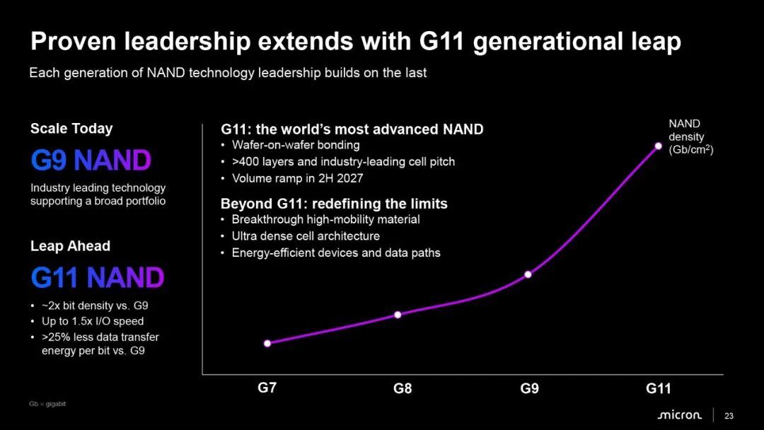
In addition to higher memory density, G11 targets a 50% higher I/O speed than G9, which means its potential transfer rate is around 5400 MT/s. In addition, Micron expects the energy consumption per bit of data transmission to be reduced by more than 25%, which is an important improvement for high-capacity solid-state drives and AI storage systems that need to process massive amounts of data.
One of the most important changes in G11 is the adoption of wafer-level bonding technology, which enables Micron to fabricate memory arrays, peripheral circuits and I/O circuits on another wafer, and then bond them together. Chinese manufacturer Yangtze Memory Technologies (YMTC) has already used this method to maximize memory capacity and performance, so it is not surprising that Micron and other memory manufacturers have also adopted this technology.
Micron expects to start mass production of G11 3D NAND in the second half of 2027.
3D NAND Beyond G11:
New Materials and Further XYZ Dimensional Scaling
Micron plans to continuously improve its 11th-generation and later 3D NAND flash technologies by combining new materials, higher-density memory cell architectures, and more energy-efficient devices and data paths. Specifically, Micron is researching high-mobility materials that can improve the electrical properties of future memory devices, as well as ultra-high-density cell architectures designed to go beyond the memory density improvements achieved by adding active layers.
At the same time, more energy-efficient circuits and data paths should help offset the growing power consumption associated with higher NAND capacities and faster interfaces.
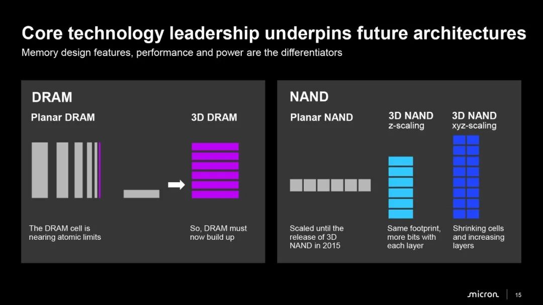
"Beyond G11, we have a strong roadmap that we will not go into detail today, but the focus is on leveraging new materials to increase the density of cell structures, and continuing to focus on XYZ scaling," DeBoer said. "The current direction of the industry and Micron's direction is to achieve scaling by adding layers and shrinking cell sizes."
The company has not disclosed which new materials it plans to introduce