DRAM technology has reached a crossroads.
Recently, the DRAM industry has presented different answers regarding the future direction of technology.
On October 9, Changxin Memory Technologies announced at the 4th Integrated Chips and Chiplets Conference in Shanghai that it is expected to launch a new generation of DDR5 RDIMM server memory that integrates 4F² architecture and hybrid bonding technology by the end of the year. Three days later, Song Jae-hyuk, CTO of Samsung Electronics' Semiconductor Division, reaffirmed at SEDEX 2026 that the company is still advancing 4F² development; SK Hynix had already written the 4F² Vertical Gate (VG) platform into its 30-year DRAM roadmap for 10nm and below at the IEEE VLSI Symposium in 2025.
However, on October 21, Scott DeBoer, President and Chief Technology and Products Officer of Micron, gave a different answer at the annual technical webinar: no 4F².
DeBoer explained that Micron has researched 4F² for more than two decades, and finally determined that this technology has no viable large-scale production path due to its shortcomings in complexity and cost.
This may not be a conventional dispute over process node iteration, but the first clear technical divergence in the decades-long single path of planar proportional scaling of the global DRAM industry. Continue to extract the last generation of architecture dividends in the two-dimensional plane, or bet on the 3D stacking route in advance? The DRAM industry has reached a strategic choice at the physical limit intersection.
What exactly is the 4F² dispute about?
From 6F² to 4F²: The underlying logic of cell scaling
The core storage cell of DRAM consists of 1 transistor and 1 capacitor (1T1C structure). The chip area occupied by the cell is usually measured by "F²", where F represents the minimum feature size of the process.
Over the past 20 years, the global mainstream DRAM has adopted the 6F² architecture, that is, a single storage cell occupies a rectangular area of 3F×2F. This layout achieves the best balance between process manufacturability, electrical performance and cost, and has been used from 80nm process to 10nm-class nodes, supporting the continuous improvement of DRAM density.
4F² is regarded by the industry as the "last step" of planar DRAM scaling — the cell area is compressed from the 3F×2F rectangle of 6F² to a 2F×2F square, with a theoretical area reduction of about one third. The prototype data displayed by Samsung at ISSCC 2026 shows that the number of dies per wafer can be increased by about 20-30%, which is the layout scheme with the highest density under the planar architecture.
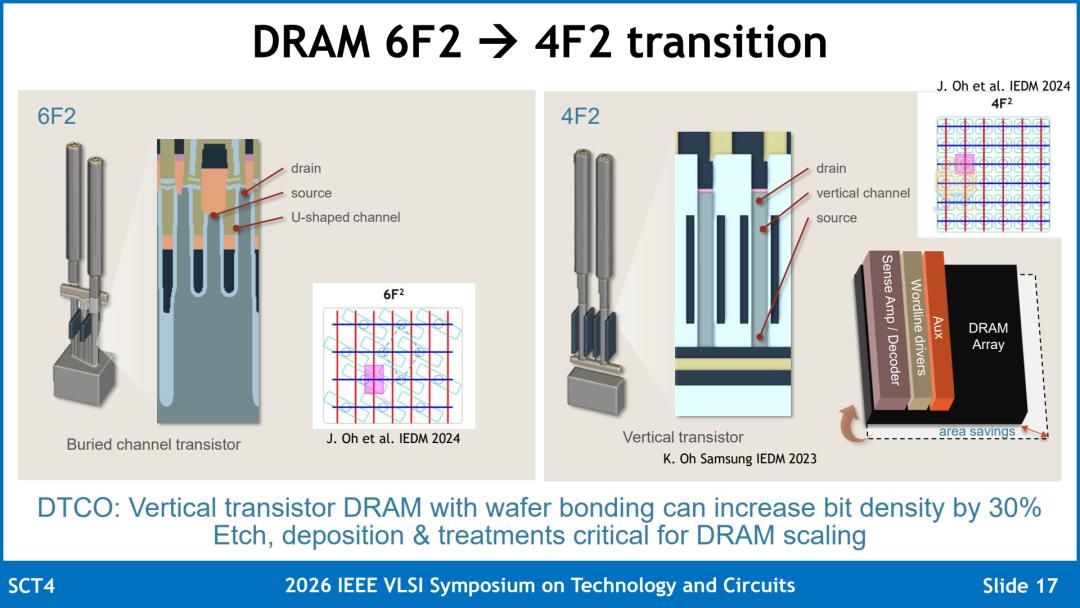
But this is by no means a simple size scaling. To realize the 4F² layout, the originally horizontally placed transistors must be erected vertically, and the effective channel length is maintained without increasing the lateral area through the vertical channel or vertical gate structure, so as to alleviate the short-channel effect and suppress leakage.
In other words, 4F² is essentially a reconstruction of the transistor architecture, not a simple lithography scaling.
Micron: 4F² has no practical benefits
However, as one of the earliest manufacturers to study the 4F² architecture, Micron's negation is extremely influential. Scott DeBoer, President and Chief Technology and Products Officer of Micron, clearly stated at the seminar: "Part of the discussion about 4F² is essentially a smokescreen. The core that determines the DRAM bit density is the capacitor pitch, not the layout of the transistors."
His core logic is: the real bottleneck of DRAM density is not the transistor, but the storage capacitor. In order to ensure reliable data storage, the capacitor must maintain sufficient charge, which determines that there is a physical lower limit for the pitch and size of the capacitor. No matter the 4F² or 6F² layout is adopted, it must finally adapt to the given capacitor pitch; although 4F² reduces the transistor area, it cannot break through the density ceiling brought by the capacitor, but will greatly increase the process complexity and manufacturing cost.
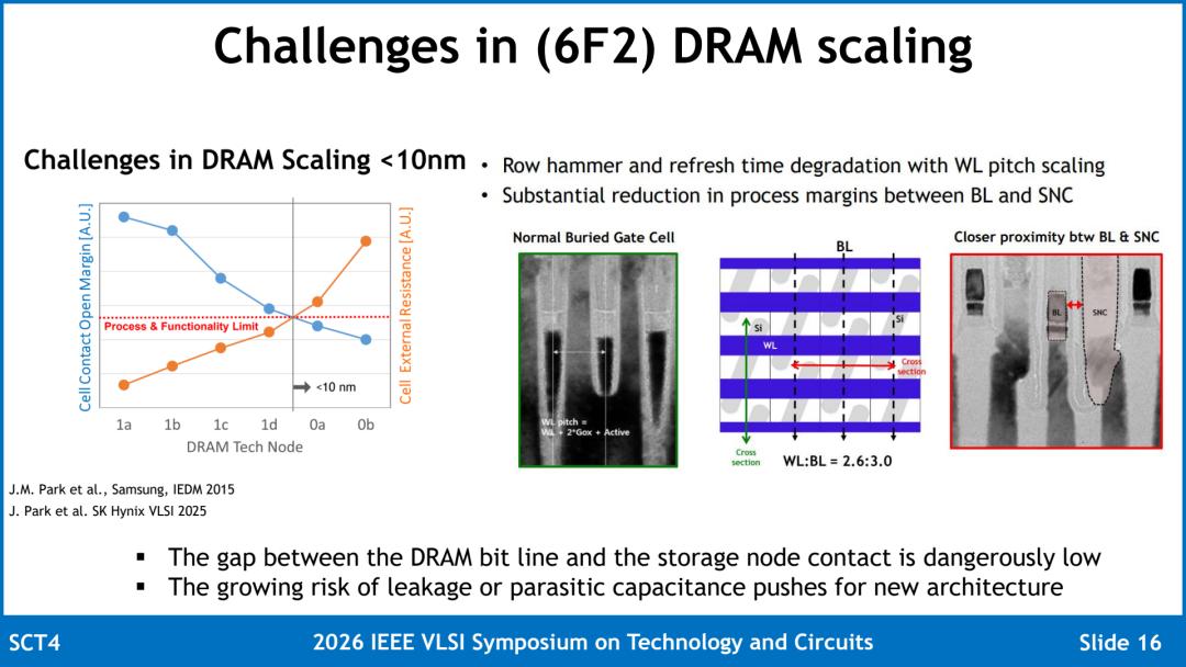
According to this logic, if the capacitor pitch cannot be reduced synchronously at advanced nodes, the density benefit of 4F² will be overestimated; while the vertical channel transistor required to realize 4F² has extremely strict requirements on the process window of atomic layer deposition and selective epitaxy, and the manufacturing cost and complexity will rise substantially.
Micron said that the company has researched 4F² for more than 20 years and has completed multiple generations of prototype verification, but the final conclusion is: there is no mass-producible large-scale scaling path, and the density benefits will be completely offset by process costs and yield losses. Therefore, Micron chose to completely abandon the 4F² route and invest all R&D resources in the continuous optimization of 6F² and 3D DRAM technology.
Samsung and SK Hynix: Continue to bet on 4F²
Contrary to Micron's judgment, the logic of Samsung and SK Hynix can be summarized as: 4F² is a necessary verification platform to get through the key process modules of 3D DRAM.
From the perspective of short-term density dividends, even if there is a capacitor bottleneck, the 4F² architecture can still achieve about 30% cell area reduction under the current process node, which is still worth promoting.
As the core direction of the next-generation planar architecture, taking the lead in mass production and establishing patent barriers can define industry technical standards and take the initiative in future competition. In addition, Samsung and SK Hynix have invested years of R&D resources in the 4F² direction, accumulating a large number of technical achievements and patents, with extremely high sunk costs; on the premise that there is no clearly better route, continuing the existing R&D rhythm is a more stable choice.
Among them, Samsung's route is the most specific. In February 2026, Samsung demonstrated a 16Gb 4F² DRAM prototype at ISSCC 2026, which integrates vertical channel transistor (VCT) and inter-wafer hybrid copper bonding technology. This is the world's first public practice combining 4F² cell structure with VCT process.
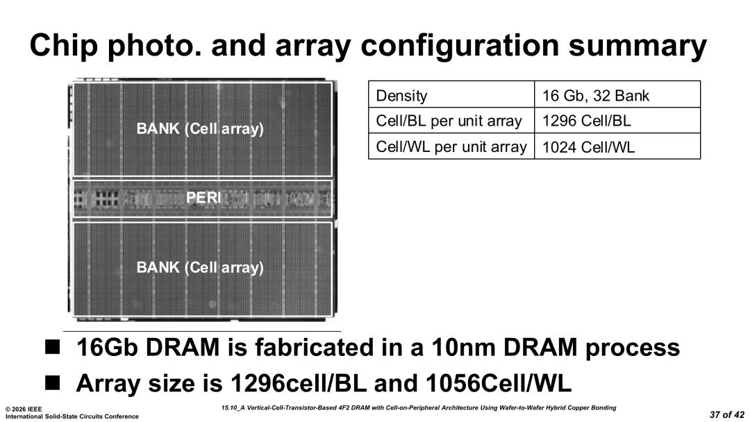
The sample demonstrated by Samsung is a 16Gb, 32 Bank VCT DRAM with 10nm process (Source: Semiconductor Industry Report)
In April, Samsung further produced working wafers below 10nm based on the 4F² architecture, with the actual circuit line width of about 9.5 to 9.7 nanometers. According to Samsung's plan, 4F² + VCT will be continuously applied to three generations of DRAM products: 10a, 10b and 10c, and will fully shift to 3D DRAM at the 10d node.
This means that Samsung positions 4F² as a process base spanning three generations: the channel formation of VCT, the alignment accuracy of wafer bonding, and the separate manufacturing of cell arrays and peripheral circuits, these capabilities required by 3D DRAM are completed under the planar architecture for yield ramp-up and process maturity. When stacking, you only need to solve the problem of stacking upwards, without facing multiple uncertainties of "new transistor structure + new integration method + new stacking architecture" at the same time.
SK Hynix's route is isomorphic to Samsung's in methodology, but with different rhythm and focus.
In June 2025, SK Hynix officially released the 4F² VG technology route at the IEEE VLSI Symposium: the gate of the transistor is placed vertically, and the channel surrounds the gate to achieve 4F² cell area. This technology integrates Bit Line Shielding (BLS) technology to suppress coupling noise, and shared Back Gate (BG) technology to enhance threshold voltage control and improve the turn-on gate effect, and cooperates with chip thinning technology to ensure the reliability of the wafer bonding structure.
SK Hynix clearly stated that the 4F² VG platform will be oriented to process nodes of 10nm and below, and is expected to achieve a bit density increase of more than 20%.
It is reported that SK Hynix plans to introduce 4F² and vertical transistors at the 10b node instead of the 10a node, which is one node later than Samsung. Part of the reason is that the development completion time at the 1d node is about 3 months later than Samsung, and the mass production preparation is about half a year later.
However, the rhythm of SK Hynix's technology verification is not slow: in July 2026, SK Hynix has verified the read and write functions of 4F² related technologies through the test array; in the same month, the bit line shielding and shared back gate structure were published on VLSI to reduce the read failure rate; and it plans to publish the "capacitor-less 4F²" design at IEDM in December, which is clearly stated to be completely compatible with the existing vertical gate DRAM process.
SK Hynix's dual-track parallel strategy takes VG as the recent density gripper and 3D DRAM as the long-term alternative, and the two share the same set of process innovations — in the words of its CTO, "Some people warn about the rising cost brought by the number of stacked layers, but this can be solved through continuous technological innovation."
The ideas of Samsung and SK Hynix can probably be understood as: the manufacturing complexity of 4F² is not a cost to be avoided, but an engineering liability that needs to be digested and mastered in advance. Skipping it means that when the 3D DRAM era arrives, the underlying capabilities such as VCT and hybrid bonding will still stay in the R&D stage, not the mass production verification stage.
Changxin Memory: The "chaser" overtaking on curves with 4F²
The progress of Changxin Memory's 4F² is a much-watched Chinese variable in this global technical divergence.
In October 2026, Changxin Memory Technologies officially announced at the 4th Integrated Chips and Chiplets Conference that it has made key breakthroughs in self-developed 4F² architecture, and a new generation of DDR5 RDIMM that integrates 4F² architecture and hybrid bonding technology will be launched at the end of 2026, officially entering the server memory market.
It is reported that Changxin's 4F² solution adopts a self-developed VSG (Vertical Surrounded Gate) transistor structure, which strengthens the gate control capability through the vertical surrounding channel design, solves the problems of leakage and short-channel effect, and at the same time achieves a significant reduction in cell area.
In terms of technology accumulation, Changxin has launched 4F² research and patent layout since its establishment. At present, there are more than 300 publicly related patent families; it published the first paper related to 4F² architecture in Chinese mainland in 2021, and continuously published R&D progress in 2023 and 2025. Its technology precipitation is not a short-term effort.
In terms of supporting processes, Changxin's fifth-generation DRAM technology platform (G5 platform) was officially mass-produced in September 2026, and the number of dies per wafer has increased by more than 50% compared with the previous generation, laying a process foundation for the implementation of 4F² products.
If the product is launched as scheduled at the end of the year, this will be the world's first mass-produced 4F² DRAM product, marking that Chinese DRAM manufacturers have for the first time achieved synchronization with international first-tier players in core architecture innovation. But it needs to be viewed objectively: server-level RDIMM has extremely high requirements for reliability and compatibility. The first-generation product is more of technical verification significance, and the mass production yield and market acceptance remain to be observed.
There are also voices in the industry that under the condition that EUV lithography equipment cannot be obtained, the conventional path of planar scaling is closed for Changxin. What 4F² provides is another density improvement channel: instead of relying on further reduction of line width, it reduces the area coefficient from 6 to 4 within the line width achievable by DUV through the reform of cell architecture.
This may also be the option and strategic consideration for Changxin to seek density breakthroughs under the condition of limited planar scaling.
3D DRAM has become inevitable
Micron: Skip 4F², go all in on 3D DRAM
After abandoning 4F², Micron's technology roadmap presents a clear path of short-term planar continuation and long-term 3D transition.
In terms of planar process, Micron's iteration rhythm remains stable:
1γ node: the first DRAM node to introduce EUV lithography, which started shipping in 2025 and is the current mass production main force;
1δ node: the 8th generation 10nm-class node, which is currently in the yield ramp-up stage and is expected to enter mass production ramp-up in 2027;
1ε node: will introduce Wafer-to-Wafer (W2W) hybrid bonding technology, adopt the Cell-on-Peri architecture, separate the storage cells and peripheral circuits on different wafers for manufacturing and then bond them, so as to improve density and performance;
The subsequent ζÅ node: plans to introduce High NA EUV lithography technology to further promote planar scaling.
In the long-term route, Micron has clearly planned two generations of 3D DRAM products, 3D1 and 3D2, as the final solution after planar scaling comes to an end. Micron said that the mass production timing of 3D DRAM will be based on business decisions, and will be officially introduced when the cost, complexity and device performance reach the optimal balance point.
On the other hand, Micron's vHBM and vEIM belong to the system-level vertical integration direction, which vertically stacks DRAM dies, base dies and logic main chips to shorten the data communication path; the first-generation vEIM targets 2TB/s bandwidth and energy efficiency lower than 1pJ/bit, and is planned to arrive in 2028, when bump-less hybrid bonding technology will be applied. This line solves the problem of bandwidth and energy efficiency, directly targeting the evolution logic of HBM, rather than the density competition of planar DRAM.
On the whole, Micron's strategy seems a bit radical. It bets that the long-term ceiling of 3D DRAM is much higher than that of 4F², but the risk is that the mass production of 3D DRAM is generally expected to be after 2028, and Micron may face continuous competitive pressure on density during the gap period from players that continue to promote 4F².
Samsung 3D DRAM has the highest number of stacked layers
As mentioned above, Samsung is one of the core promoters of the 4F² route, and it is also simultaneously deploying in the direction of hybrid bonding and 3D stacking, adopting a multi-line parallel strategy.
In terms of 4F² technology, Samsung has chosen the vertical channel transistor (VCT) path, which alleviates the short-channel effect by increasing the channel height, and at the same time introduces IGZO oxide semiconductor materials to suppress leakage, making its 16Gb 4F² DRAM prototype have a cell area 33% smaller than that of 6F². At the same time, Samsung is also adjusting its technical priority to formalize the hybrid bonding solution. Its B1b hybrid bonding solution adopts the Cell-on-Peri architecture. The memory array and peripheral circuits are manufactured on separate wafers and then integrated through copper hybrid bonding, which can relax design rules, improve overall density, and the commercialization threshold is lower than that of the pure VCT solution.
In the