Optical chips have ushered in an inflection point.
In 2026, the optical chip industry is embracing a new round of development boom.
Recently, global semiconductor giants have taken frequent actions.
In mid-October, Intel showcased the latest progress of silicon photonics technology at the OCP Global Summit, focusing on promoting the integration of InP lasers and 300mm silicon photonic wafers; Samsung is also speeding up its pace, planning to launch silicon photonics foundry services in 2027; UMC announced an additional capital expenditure of about 3.2 billion US dollars, listing silicon photonics as one of the key capacity expansion directions.
On the other side, Tower Semiconductor has obtained tangible orders. In May this year, Tower announced that it had signed a silicon photonics customer contract corresponding to 1.3 billion US dollars in revenue in 2027, and in September, it announced that 800G to 1.6T laser-integrated optical chips had begun mass shipment.
It is not only the chip manufacturing end that is bustling, but the application end has also started to show momentum. Since the beginning of this year, NVIDIA Spectrum-X CPO switches and Broadcom 51.2T Bailly CPO switches have successively entered the limited-scale shipment stage, which means that the previously highly concerned co-packaged optics technology is gradually moving out of the laboratory and entering actual commercial applications.
Giants that were originally located in different links of the semiconductor industry chain are accelerating convergence in the field of optical chips. The strategic value of optical chips is also gradually evolving from traditional data transmission devices to key technologies that affect the architecture, energy consumption and even future expansion methods of AI computing systems.
Optical Chips Move to the Center of the Stage
To understand this round of optical chip boom, we first need to clarify a concept: what manufacturers such as Intel, Samsung and TSMC are focusing on deploying at present is not "optical computing chips" that directly use photons to complete neural network calculations, but photonic integrated circuits (PICs) and optical interconnection chips that use optical signals to transmit data.
Although both belong to photonics technology, their commercialization paths are completely different. The former aims to change the computing mode, while the latter focuses on solving a more realistic problem: as AI chips become more and more powerful, how to make the data exchange between them keep up with the computing speed?
Over the past decades, the semiconductor industry has continuously improved performance by increasing transistor density, expanding chip area and adding computing units. However, as AI clusters expand from thousands of accelerators to a larger scale, the growth of computing power begins to be restricted by communication capabilities.
This is also why in recent years, NVIDIA has not only continued to improve GPU performance, but also vigorously expanded the NVLink network, while HBM and advanced packaging have also been pushed to the forefront of industrial competition. Essentially, they are all solving the same type of problem: how to make data reach the computing units that need them with higher efficiency.
But these technologies cannot completely solve all data transmission problems.
In the internal connection of chips and the inter-chip connection of extremely short distance, electrical interconnection still has obvious advantages by virtue of mature technology, low cost and high integration density. However, when the transmission rate continues to increase, especially when the single-channel rate evolves from 100Gbps to 200Gbps and 400Gbps, the insertion loss, signal integrity and power consumption problems of copper interconnection begin to become more prominent.
In order to maintain high-speed signal quality, the system must invest more resources in equalization, retiming and signal driving. These auxiliary circuits not only consume extra power, but also increase delay, area and system design complexity.
In contrast, optical signals have lower propagation loss during long-distance transmission, and can use Wavelength Division Multiplexing (WDM) to allow light of different wavelengths to transmit data in parallel in the same optical fiber.
In August 2026, a review published in *Nature Electronics* specifically discussed this trend. The research points out that electrical interconnection is facing constraints such as resistance loss, capacitive load and frequency-dependent distortion, while optical computing interconnection is expected to provide new development space in terms of bandwidth, energy consumption and signal integrity.
The problem is that light is not naturally more economical than electricity.
Optical interconnection must complete electro-optical conversion and photoelectric conversion, which requires lasers, modulators, photodetectors and corresponding electronic driving and receiving circuits. If the connection distance is short enough, the power consumption and cost brought by the photoelectric conversion itself may completely exceed the overhead saved by using optical fibers.
Therefore, the value of optical chips does not lie in completely replacing copper interconnection, but in finding a critical point: when bandwidth, distance and power consumption reach a certain scale, the comprehensive benefit of optical interconnection begins to exceed that of electrical interconnection.
An intuitive change is that the position of photoelectric conversion is constantly moving closer to the computing chip.
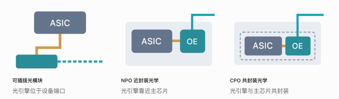
A simplified schematic diagram of the evolution direction of the optical interconnection architecture, not a proportional engineering structure. Gray represents computing/switching chips, cyan represents optical engines, gold represents short-distance electrical connections, and cyan lines represent optical connections. The specific structures of NPO and CPO vary from manufacturer to manufacturer.
Traditional pluggable optical modules are installed on the switch panel, and high-speed electrical signals need to pass through the packaging and PCB traces from the switching chip to reach the module. NPO and CPO reduce signal loss and electrical interface power consumption by shortening this section of high-frequency electrical connection.
If traditional optical communication solves the problem of how to communicate between data center devices, CPO is trying to further solve the problem of how to communicate efficiently between chip packages and even multi-rack computing systems. As a result, optical chips have begun to enter the core competition field of semiconductor manufacturing and advanced packaging.
Intel, Samsung, TSMC are Competing for Different Industrial Entries
Although all regard silicon photonics technology as an important direction for the future, a careful study of the layouts of Intel, Samsung and TSMC shows that there are obvious differences in the three companies' technology accumulation, entry positions and business objectives.
Intel: Trying to Solve the Most Basic Light Source Problem of Optical Chips
Intel is not a new player in this competition.
As early as more than 20 years ago, Intel began to invest in silicon photonics technology R&D. According to the data disclosed by its official, since 2016, the company has shipped more than 8 million photonic integrated circuits, and more than 32 million lasers integrated on these chips. Therefore, compared with many manufacturers that are still in the R&D or sample verification stage, Intel already has a certain scale of silicon photonics manufacturing experience and light source reliability accumulation.
Silicon photonics technology has long faced a basic problem: silicon is very suitable for manufacturing waveguides, modulators and other optical structures, but it is not an efficient luminescent material. To generate laser on a silicon photonic chip, it is usually necessary to introduce III-V compound semiconductors such as indium phosphide, or supply light to the chip through an external laser source.
One of the main directions chosen by Intel is to use heterogeneous material integration to combine InP materials with silicon photonic wafers, and then manufacture laser structures through wafer-level processes.
At the 2026 OCP Summit, Intel further emphasized that it has the ability to manufacture InP integrated light sources for 300mm silicon wafers, aiming to reduce the complexity of light source manufacturing and integration by leveraging the scale advantage of large-size silicon wafer processes. It needs to be emphasized here that this is not manufacturing lasers on 300mm pure InP wafers, but integrating InP materials into the 300mm silicon photonics manufacturing platform. There are obvious differences between the two in material technology and commercial significance.
Intel hopes to solve two key problems through this: first, reduce the precision optical coupling link between the external laser and the optical chip, and second, bring more laser manufacturing, testing and burn-in screening into the wafer-level process, so as to improve the consistency of large-scale manufacturing.
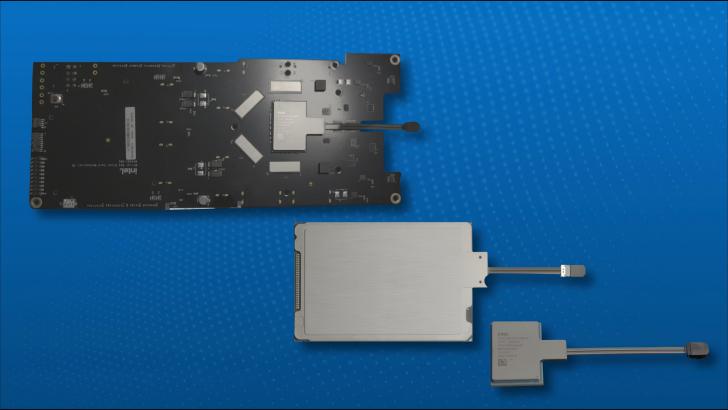
Its latest Optical Compute Interconnect (OCI) Chiplet solution also reflects this direction. This solution combines PIC containing on-chip lasers with advanced CMOS electronic chips. The first generation has a bidirectional bandwidth of 4Tbps, and the goal is to be co-packaged with computing chips such as CPUs and GPUs without a separate external laser light source.
Intel's real advantage may not just be manufacturing faster optical chips, but trying to turn silicon photonic devices and integrated light sources into standardized semiconductor products that can be mass-produced and screened at the wafer level.
But integrated light sources also have costs. After the laser enters the vicinity of the high-power consumption computing chip, it will face a more complex thermal environment, and at the same time lose part of the advantage that the external light source is easy to replace separately. Therefore, on-chip laser is not an inevitable choice for all CPO systems.
For Intel, its biggest challenge is how to further transform its long-accumulated technical capabilities into mass-deliverable optical interconnection products and foundry services, instead of only staying at the technology verification stage.
Samsung: Incorporate Optical Chips into the Integrated Strategy of Storage, Logic and Packaging
Different from Intel, Samsung's entry point is more inclined to the complete semiconductor manufacturing and packaging system.
In March 2026, Samsung officially demonstrated the silicon photonics foundry business roadmap at the OFC conference, announcing that it has preliminary production readiness including Process Design Kit (PDK), and plans to manufacture PICs with 300mm wafers. Its subsequent roadmap includes introducing thermocompression bonding optical engines in 2027, upgrading hybrid copper bonding technology in 2028, and planning a full CPO turnkey service in 2029.
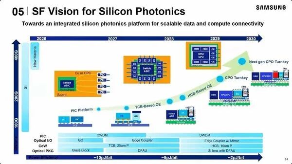
The optoelectronic integration roadmap proposed by Samsung aims to further integrate PIC, EIC and switching chips, and finally expand to computing systems where GPU, XPU and HBM are co-packaged.
By September, Samsung further increased the construction of optoelectronic testing capabilities. According to a report from *The Elec*, the company is using probe testing equipment from FormFactor and MPI to conduct internal evaluation of PIC wafers, hoping to complete relevant verification work by the end of 2026.
Another important bargaining chip for Samsung is its storage business.
In the traditional AI accelerator industry chain, advanced logic chips, HBM and advanced packaging often involve collaboration between different enterprises. Samsung has a combination of storage, logic wafer foundry and packaging technologies, and can try to provide manufacturing solutions with a higher degree of integration. From a business strategy perspective, Samsung is betting on a potential change: in the future, AI chip customers may no longer just purchase advanced process wafers, but comprehensive manufacturing services including logic, storage, optoelectronic interconnection and packaging.
If this direction is established, Samsung will have the opportunity to use silicon photonics technology to fill an important link in its integrated AI semiconductor services. However, this still depends on whether external customers can actually adopt its manufacturing platform. Having multiple manufacturing capabilities does not automatically equal the ability to provide competitive system-level products.
TSMC: Make Optical Chips Part of Advanced Packaging
Compared with Intel and Samsung, TSMC's route is more direct: through the mature wafer foundry and advanced packaging ecosystem, it takes photonic chips as a new heterogeneous integration unit.
TSMC has previously established a 65nm silicon photonics process platform, and developed technology for three-dimensional stacking of electronic integrated circuits and photonic integrated circuits.
In April 2026, TSMC announced at the North American Technology Symposium that its Compact Universal Photonic Engine (COUPE) technology will usher in an important node: the co-packaged optics solution using the COUPE optical engine on the substrate is scheduled to start production in 2026. TSMC said that compared with the pluggable solution on the circuit board, its co-packaged architecture can improve power efficiency by about 2 times and reduce latency by about 10 times.
TSMC's advantage is that it can develop COUPE in coordination with its existing 3DFabric advanced packaging system.
In the past, the core task of advanced packaging was to connect logic chips with HBM to improve the efficiency of data exchange within the package. Now, if the optical engine also enters this system, the function of the package will no longer be limited to connecting chips in the same package, but also undertake part of the task of outputting high-speed data to external computing nodes. As optoelectronic interconnection enters the advanced packaging system, the competition boundary between optical chip manufacturing capabilities and packaging capabilities is becoming blurred.
For TSMC, optical chips do not necessarily need to use the most leading process like advanced logic chips. Even if a relatively mature silicon photonics process is adopted, as long as it can be integrated with advanced CMOS, 3D stacking and high-density packaging, it can still form high system value.
The future industrial competition may not be a simple silicon photonic wafer manufacturing competition between Intel, Samsung and TSMC, but a competition for different enterprises to build a complete ecosystem around optical engines, electronic chips, light sources, optical fiber interfaces and advanced packaging capabilities.
This is why GlobalFoundries has also increased its investment. On July 29, 2026, GlobalFoundries announced that it had signed a letter of intent with the U.S. Department of Commerce, and is expected to receive 300 million US dollars in R&D funds under the CHIPS and Science Act to promote the R&D of new silicon photonic materials, wafer technologies and advanced packaging, focusing on NPO and CPO.
It is not difficult to see from this that silicon photonics competition is not only a device innovation, but also has begun to become an important extension for wafer foundries to compete for future high-performance computing business.
UMC and Tower: Optical Chips Enter the Capacity Competition
With the accelerated commercialization of silicon photonics technology, traditional wafer foundries have also begun to increase investment. Different from Intel, Samsung and TSMC which focus on optoelectronic integration and advanced packaging, UMC and Tower Semiconductor are relying on mature processes, special processes and large-scale manufacturing capabilities to compete for the fast-growing optical chip foundry market.
On October 28, UMC announced an additional capital expenditure budget of about 3.2 billion US dollars to accelerate the capacity construction of emerging businesses such as silicon photonics and advanced packaging. According to the plan, the company plans to expand the monthly production capacity of silicon photonics to about 18,000 wafers, and at the same time build a monthly production capacity of about 20,000 wafers for thin-film lithium niobate (TFLN) modulators. The relevant new capacity is expected to start ramping up at the end of 2028 and reach the planned scale in 2030.
UMC's layout has achieved initial commercial progress. In July this year, UMC and Singapore's SILITH Technology announced that the silicon photonic chips jointly developed by the two parties had achieved the first batch of mass-produced wafer delivery at UMC's 12-inch fab in Singapore, mainly for 1.6T high-speed optical interconnection applications. At the same time, UMC is promoting single-channel 400G silicon photonics technology, and cooperating with enterprises such as HyperLight to lay out the TFLN manufacturing platform to further improve high-speed optical modulation capabilities.
Compared with UMC's large-scale capacity expansion, Tower Semiconductor, another special process wafer foundry, has presented more direct commercial achievements.
In May this year, Tower announced that it had signed a contract with major customers corresponding to 1.3 billion US dollars of silicon photonics business revenue in 2027, and received 290 million US dollars in customer prepayments to lock in manufacturing capacity in advance. The company also revealed that the committed scale of contracted wafer demand in 2028 has further expanded, and the number of active silicon photonics customers has exceeded 50.
In terms of products, Tower announced in June this year that the cumulative shipment of coherent photonic integrated circuits produced in cooperation with Marvell has