The landscape of chip manufacturing has been reshaped.
In the past, the semiconductor industry chain operated under a well-defined division of labor model: chip design companies were responsible for product definition, wafer foundries took charge of manufacturing, and packaging and testing plants undertook subsequent processing, with all links connected via orders and unified technical standards. However, the explosive growth of AI computing power demand has broken the traditional operating rules of the chip manufacturing industry.
Chips are getting larger in size, and the complexity of advanced processes and advanced packaging keeps rising. The smooth delivery of an AI chip no longer depends solely on a single production link. Wafers, HBM, packaging substrates, and testing can all become restrictive factors. This means that AI chip manufacturing can no longer be simply completed step by step relying on the original division of labor. Driven by the urgent demand for computing power, the entire industry chain is reshaping its production logic.
Why the Traditional Division of Labor Is Starting to Fail
As the scale of large AI models continues to expand, AI chips require stronger computing power, higher memory bandwidth, and more efficient inter-chip interconnection. Relying solely on transistor miniaturization can no longer meet all performance requirements. Advanced processes, HBM memory and advanced packaging now jointly determine the upper performance limit of an AI chip.
Take Nvidia's Blackwell architecture as an example. Its GPU adopts a dual-die design, integrating two dies into one computing unit through high-speed interconnection, and is paired with high-bandwidth memory to provide data throughput capability. This kind of design can further increase the computing scale, but also makes the manufacturing process more complex.
Source: TrendForce
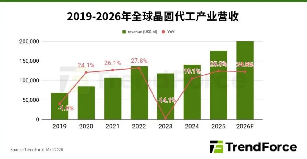
While the complexity of AI chips is rising, market demand is also being released rapidly. TrendForce estimated in March 2026 that the global wafer foundry industry's full-year revenue will increase by 24.8% year on year to reach about 218.8 billion US dollars; among them, the production capacity of TSMC's 5/4nm and more advanced processes will remain fully loaded by the end of 2026. What is driving this round of high-capacity operation is exactly the AI GPUs from Nvidia and AMD, as well as self-developed chip orders from cloud vendors and AI enterprises such as Google, AWS and Meta.
The packaging segment is also facing similar pressure. The size and packaging area of AI chips continue to increase, and the wafer and packaging resources consumed by a single chip rise accordingly. The production capacity of 2.5D advanced packaging such as CoWoS has been continuously tight since 2023, and the supply pressure has also spread to the fields of packaging equipment, substrates and key materials. Even if wafer fabs continue to expand production, the final delivery will still be affected as long as packaging or other key components cannot keep up synchronously.
Therefore, under the traditional model, the industry chain's "each taking charge of its own segment" can no longer withstand this highly coupled production complexity, and the old industry conventions have thus loosened. At present, all links in the industry chain are forced to make choices different from past practices.
Chip Companies No Longer Only Focus on Design
In the past, under the mature "Fabless + Foundry" model, chip design enterprises were only responsible for product specification definition and circuit scheme design, while manufacturing was handed over to external wafer fabs and packaging and testing plants. However, at present, advanced manufacturing resources are in short supply, and relying solely on placing orders is no longer enough to lock in a stable supply. Therefore, leading customers have begun to get involved in suppliers' resource planning in advance through long-term agreements, capacity reservation, advance payments and other methods.
Source: Nvidia
In July 2026, Amkor signed a 1.5 billion US dollar multi-year advanced packaging and development agreement with Nvidia. Nvidia paid an advance payment to support Amkor to expand its advanced packaging capacity in the United States. On October 21 of the same year, the two sides officially announced another cooperation project for capacity expansion in South Korea, and the total amount of relevant agreements in the US and South Korea reached 3 billion US dollars.
Similarly, similar arrangements have emerged in the testing segment. Nvidia provided 1.1 billion US dollars in capacity reservation advance payment to King Yuan Electronics to fund the construction of a testing factory in the United States and the procurement of production equipment, with the mass production target of the project set for April 2027. In the substrate supply chain, on October 21, Nvidia announced cooperation with Ibiden, Samsung Electro-Mechanics and XinXing Electronics, planning to increase the relevant substrate production capacity to 2.5 times the current level in the next three years; among them, Ibiden's expansion of its Ono Plant in Japan also received support from Nvidia's capacity reservation advance payment.
This series of cooperation shows that chip design companies have begun to participate in the expansion and capacity allocation of manufacturing suppliers through capital and long-term demand commitments. Suppliers get clearer demand signals, while customers secure more guaranteed manufacturing resources. The connection between chip design and manufacturing has become unprecedentedly close, and the cooperation boundary between the two has extended to the level of capacity construction and medium and long-term capacity planning.
However, this model will also amplify the polarization in the industry. Leading enterprises with sufficient capital and the ability to commit to large long-term orders can take priority to seize scarce production capacity. For small and medium-sized manufacturers with weak capital strength and bargaining power, it will become more difficult to obtain priority supply qualification.
Competitors Start to Do OEM for Each Other
Locking production capacity through advance payments can improve the certainty of supply, but the construction of new production lines and process verification both require cycles, and manufacturing capacity cannot be expanded out of thin air in a short time. Facing the persistently high market demand, AI chip-related enterprises have begun to look for external production capacity, and hand over part of the production links to peers that originally belonged to the competitive camp.
On October 8, GlobalFoundries signed a five-year long-term manufacturing agreement with TSMC with a total amount of about 2 billion US dollars. GlobalFoundries will supply silicon interposers for TSMC's CoWoS advanced packaging ecosystem at its factory in Malta, New York, and the project is expected to gradually enter mass production in the first half of 2028. TSMC and GlobalFoundries were originally competitors in the wafer foundry track, but in this cooperation, GlobalFoundries changed its identity to undertake manufacturing supporting work for TSMC's advanced packaging ecosystem.
This cooperation reflects that the division of labor in the chip manufacturing industry chain is being reshuffled. TSMC makes up for the supply of silicon interposers through external procurement, concentrating its own resources on the core advanced process and packaging business; GlobalFoundries revitalizes its existing manufacturing capacity and enters the high-growth track of AI advanced packaging. The two sides do not give up competition, but re-split specific processes based on their respective technical reserves, capacity conditions and cost considerations.
Similar changes in division of labor can also be seen in the HBM supply chain. According to a report by *The Seoul Economic Daily* on October 18, 2026, Nvidia is cooperating with Samsung and TSMC to develop customized high-bandwidth memory NVHBM, and the logic chip of the memory base is planned to be produced using TSMC's 3nm process.
If the solution in the report is implemented, it means that different manufacturing links of an HBM product can be completed by multiple enterprises based on their respective technical and capacity advantages. When enterprises choose cooperation partners, their considerations are no longer limited to whether there is a competitive relationship between them, but also include the technical capabilities, capacity conditions and delivery efficiency required for specific processes.
Wafer Foundries and OSATs Are Competing for the Same Market
The trend of breaking the original industry boundary has also spread to the fields of wafer foundry and packaging and testing. As AI chips increasingly rely on multi-chip integration and high-bandwidth memory, advanced packaging has continuously raised requirements for interconnection density and fine circuits, and its processes have begun to move closer to wafer manufacturing. For example, the manufacturing of Redistribution Layer (RDL) requires more complex photolithography technology to form finer circuit structures. At the same time, wafer foundries are facing pressure on capacity allocation and need to prioritize securing advanced process businesses, leaving space for professional packaging and testing plants to undertake part of the back-end processes. As a result, wafer fabs and packaging and testing plants have begun to enter the same market.
TSMC is the representative of this change. As the leader of wafer foundry, TSMC integrates logic chips and high-bandwidth memory into the same packaging through technologies such as CoWoS, and incorporates advanced packaging into the 3DFabric technology system. This means that advanced packaging is no longer the exclusive business of packaging and testing plants.
On the other hand, packaging and testing enterprises represented by Amkor are gradually mastering part of the back-end manufacturing capabilities that were previously mostly undertaken by wafer foundries. According to official disclosure, Amkor has long laid out 2.5D packaging and jointly developed the H-Cube solution for high-performance computing and AI chips with enterprises such as Samsung. The company's management also stated that as relevant technologies mature, technologies such as 2.5D packaging, micro-bumps and wafer-level fan-out packaging may gradually enter the business scope of OSATs.
However, the blurring of business boundaries does not mean that the two sides can only replace each other. In 2024, TSMC and Amkor announced cooperation to plan to establish a closer advanced packaging and testing collaboration model in Arizona, USA; in 2026, the two sides announced the signing of a ten-year agreement to further promote the construction of local advanced packaging capabilities. According to the cooperation arrangements announced by the two sides, TSMC is responsible for advanced wafer manufacturing, and Amkor undertakes the corresponding packaging and testing services. The two enterprises provide customers with seamless connection from wafer manufacturing to packaging and testing through closer cooperation.
It can be seen that advanced packaging does not bring about simple business substitution, but a redefinition of the boundary between wafer foundries and packaging and testing plants. Even if competition may arise in some high-end links, production capacity and technology will prompt the two sides to continue to cooperate.
Manufacturing Processes Are No Longer Only the Concern of Wafer Fabs
The change of the division of labor model is not only reflected in who should produce the components, but also in how manufacturing technologies are developed and iterated.
In links such as computational lithography, defect inspection and process control, a large amount of computing resources and complex software tools are required. In the past, after chip design companies submitted the layout files, the debugging and optimization of manufacturing processes were basically the work of wafer fabs and equipment manufacturers. Nowadays, the computing power platforms and AI tools in the hands of design enterprises are also deeply involved in the whole manufacturing process.
In May 2026, Nvidia and TSMC announced cooperation to apply Nvidia's accelerated computing and AI technologies to semiconductor design and manufacturing links. TSMC uses Nvidia's CUDA-X library and AI models to optimize computational lithography operations, transistor and process simulation, advanced process control and wafer fab operation optimization. In the defect inspection segment, technologies such as Nvidia Metropolis and TAO Toolkit are also used to promote the visual AI inspection capability.
The role of computational lithography is to convert chip design graphics into photomasks. The more advanced the process node is, the more the computational workload multiplies. According to public information from Nvidia, compared with the traditional CPU solution, its GPU-accelerated cuLitho computational lithography library can improve cost efficiency or processing cycle by 20%-50% under the same total cost of ownership, and its cuEST library can achieve an average of about 50x acceleration in chemical simulation scenarios.
Through this cooperation, the capabilities of chip design enterprises have truly extended to the manufacturing technology optimization link. Nvidia provides computing platforms, software tools and AI capabilities, while TSMC applies these capabilities to its own R&D and production processes. The two sides have formed technical synergy, which has gone beyond the ordinary supply-demand relationship between Party A and Party B.
Of course, this does not mean that AI can replace the process experience accumulated over many years. Advanced processes still rely heavily on equipment, materials, process accumulation and massive verification. The real change is that manufacturing enterprises have begun to incorporate external accelerated computing and AI capabilities into their R&D and production toolchains, so as to shorten the simulation analysis cycle, improve inspection efficiency, and assist the optimization of complex production processes.
Closing Remarks
For the chip manufacturing industry, the successive breaking of old industry rules essentially stems from the unprecedented requirements that AI chips put forward for manufacturing complexity and production capacity scale, which have exceeded the capability ceiling of a single link or a single enterprise. The traditional industrial division of labor order has thus loosened, and a brand-new cooperation model adapted to the AI era is developing closely around the needs of AI chip enterprises.
As the connections between all links in the industry chain become increasingly close, the semiconductor industry is shifting from the relatively fixed division of labor model in the past to a more flexible, open and integrated networked cooperative relationship. In the future, while consolidating their own technical and capacity advantages, enterprises also need to establish an indispensable position in industrial cooperation.
This article is from the WeChat Official Account "Semiconductor Industry Observation" (ID: icbank), written by Xia Xue, and officially released by 36Kr with authorization.