The do-or-die race of China's optical chips under the shadow of FCC
When the AI computing infrastructure boom pushes light to the center of the storm, optical chips, known as "the heart of photoelectric conversion", are naturally regarded as the next hundred-billion-level blue ocean market. From 10G to 800G, then to 1.6T and 3.2T, with each iteration of the transmission rate, the value and market space of optical chips are continuously elevated.
After years of lying dormant, China's domestic optical chip industry is gearing up, taking it as another core battlefield for domestic substitution following the semiconductor sector.
When the primary and secondary market financing boom reached its peak, a cold splash of reality came: on one hand, the shadow of FCC's restrictions on the optical interconnection industrial chain lingers, and regulatory risks extending from end modules to upstream chips keep escalating; on the other hand, the inherent manufacturing barriers, production capacity bottlenecks and yield ramp-up difficulties of optical chips are significantly more prominent than the market's previous optimistic expectations.
01 The Once-Perfect Logic: Why Are Optical Chips Regarded As A Golden Track?
I. The Prospect of Optical Chips Is Extremely Bright
Optics is the segment with the most obvious inflation attribute and the highest certainty in AI infrastructure, without exception.
Both large model training and inference highly rely on frequent, large-scale data exchange between GPUs in the cluster, making the interconnection bottleneck more prominent. Therefore, no matter how the technology of other tracks evolves, optics will always benefit. This logic was condensed into one sentence in the second quarter of this year — stand in the light, believe in the light.
From the perspective of industrial logic, this statement is correct.
A frequently cited data point shows that computing power increases by about 3 times every two years, memory bandwidth by about 1.6 times, while interconnection bandwidth only increases by about 1.4 times — this is the famous "I/O Wall". When multiple GPUs work in coordination, transmission becomes the bottleneck, and data handling efficiency becomes the core factor restricting the release of computing power.
With the advantages of high bandwidth, low latency and low power consumption, optical interconnection has become the core solution to break through the I/O Wall, which is the so-called "Optics in, Copper out". As the core semiconductor component that realizes mutual conversion of photoelectric signals, optical chips are located at the most upstream of the optical communication industrial chain, directly determining the transmission rate, power consumption, integration and reliability of optical modules.
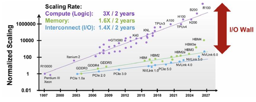
Figure: Schematic Diagram of the I/O Wall Problem Source: Soochow Securities
With the rapid growth of AI demand for optical modules and rapid technological iteration, optical chips have become the production capacity bottleneck of the entire industrial chain, and also the link with the most concentrated value.
From the perspective of BOM breakdown, optical chips account for more than 30% of the cost of optical modules, and with the iteration of rate to 800G/1.6T/3.2T, the proportion is expected to continue to rise to 60%. The gross profit margin of high-end optical chips can reach 50%–90%, which is significantly higher than the optical module assembly link.
The global laser chip market also shows an explosive growth trend, with the market size growing from USD 2.6 billion in 2024 to USD 22.9 billion in 2030, with a CAGR as high as 44.1%. If all categories of optical chips such as modulators and detectors are included, the overall market space will be broader.
It is for this reason that whether in the US stock market or A-share market, the highest valuations are all in the optical upstream sector.
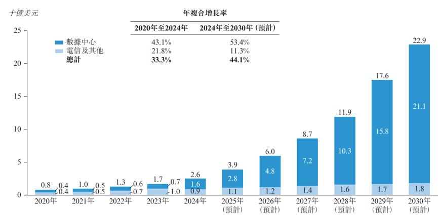
Figure: Global Optical Chip Market Size Source: Prospectus of Source Photonics for Hong Kong Stock Listing
II. Under the Shadow of FCC, Optical Chips Suffer the Greatest Valuation Impact
Not only does the optical chip industry have strong growth resilience, domestic enterprises previously had an additional logic of domestic substitution. The epic-level shortage in the global optical upstream sector has given many domestic enterprises a historic opportunity for product introduction.
Under the shadow of the US FCC (Foreign Direct Product Rule), optical chips are the most affected segment, and the future imagination space has been greatly compressed, which can be fully understood from the BOM breakdown and the current situation of the domestic industrial chain.
The core of electrical chips are DSP and some analog chips, which account for a high proportion of cost, but domestic enterprises cannot produce them at present, so they basically have no impact on domestic industrial companies.
The next highest proportion of cost is optical chips, followed by optical devices. Optical chips account for more than 30% of the cost of optical modules, and with the iteration of rate to 800G/1.6T/3.2T, the proportion will further increase in the future.
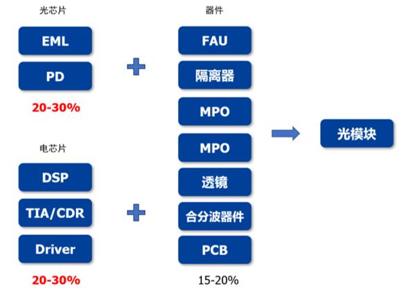
Figure: Schematic Diagram of Value Breakdown of Optical Module Industry Source: Guosheng Securities
The following is a brief analysis of the competitiveness of China's domestic optical industry chain:
There is no need to elaborate on the optical module assembly link. Chinese enterprises have the highest global market share and the strongest competitiveness, and it is difficult to get rid of the Chinese supply chain in a short period of time;
The next is optical devices. Although they are not as prominent as optical modules, many companies are suppliers of overseas Corning and Fabrinet, so their strength is not weak;
Then there are the optical chips focused on in this article, which have a very low localization rate and are also areas that need urgent breakthroughs, and the breakthrough progress was relatively fast previously;
As for electrical chips such as DSP, China has basically given up on independent development, and the attention to this segment is very low.
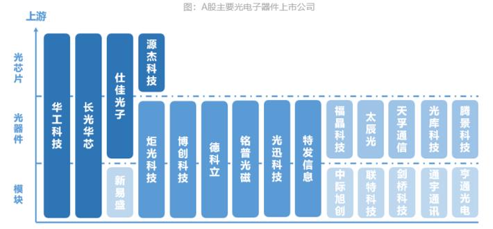
Source: AVIC Securities
02 The Truth of Manufacturing: The Difficulties of Optical Chips Are Different From What You Think
I. Optical Chips Are More Like SiC Than Electrical Chips
Judging literally, many people will analogize optical chips to "the optical version of electrical chips", thinking that as long as they follow the path of semiconductor development, they can gradually achieve breakthroughs.
But in fact, the manufacturing logic of optical chips is very different from that of electrical chips. It is a typical industry characterized by "process-driven, yield-oriented, asset-heavy and long-cycle". In other words, optical chips are not reduced versions of electrical chips, but an alternative track of precision manufacturing.
Divided by functional dimension, optical chips can be divided into active optical chips and passive optical chips. Among them, high-speed active optical chips are the link with the highest technical barriers, and also the core pain point of current localization. Since the material requirements are different from those of electrical chips (which are all manufactured on silicon), optical chips are also often divided according to material systems.
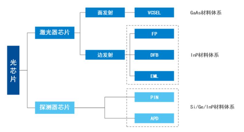
Figure: Classification of Active Optical Chips
Different from electrical chips that pursue shrinking process size, the performance improvement of optical chips does not fully rely on size reduction, but pays more attention to epitaxial structure design and growth. To a certain extent, it is closer to silicon carbide (SiC), so it places great emphasis on materials and processes.
Its production covers four major links: substrate manufacturing, epitaxial growth, wafer device manufacturing, and packaging and coupling. The overall process is not very long compared with electrical chips, but the epitaxy and grating processes require nanometer-level precision, with extremely narrow process windows and extremely difficult yield improvement.
This also directly leads to differences in industrial models: optical chip manufacturers generally adopt the IDM model, covering the whole process of design, manufacturing, packaging and testing. The IDM model means higher entry barriers — large upfront capital expenditure, the need to cover the full-process production lines from design to packaging and testing, and stable mass production and yield control capabilities. Therefore, when the annual demand was relatively limited in the past, there were very few players in this industry.

Figure: Optical Chip Manufacturing Process Source: Yunling Optoelectronics
This technical feature also makes the entire industry present three distinct characteristics:
First, the superposition of technology intensity and capital intensity. The investment in a complete InP material optical chip production line can reach tens of billions of yuan, and the core equipment relies on imports with a long delivery cycle;
Second, the scale effect comes from yield rather than output. For the same production line, when the yield increases from 30% to 60%, the cost can be reduced by half;
Third, the customer certification cycle lasts for about 2 years, which needs to go through the whole process of internal testing, module manufacturer verification, end customer certification and then mass production landing. The customer stickiness is extremely strong, and it is extremely difficult for new manufacturers to enter the supply chain.
II. Core Products Are EML and CW Lasers
At present, the core products of high-speed optical chips are EML and CW lasers, which also occupy the main future market of optical chips.
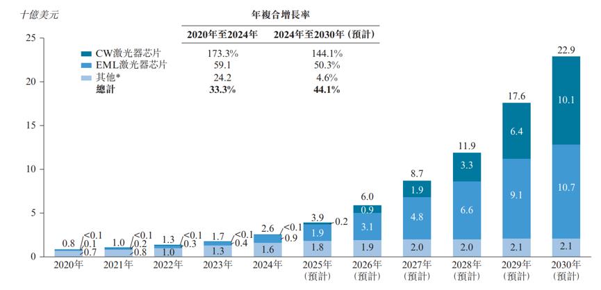
Figure: Global Optical Chips Divided By Technical Route Source: Prospectus of Source Photonics for Hong Kong Stock Listing
EML chips are known as the Mount Everest of high-end manufacturing, which requires monolithically integrating DFB lasers and EAM modulators on the same indium phosphide (InP) chip. The process complexity is significantly higher than that of CW lasers, and its mask steps are more than twice that of standard CW. The yield of high-speed products may drop from 50% to 15%.
The process complexity of 200G EML is about 2.5-3 times that of 100G, and the wafer-level yield of some products is only 10%-20%.
At present, the global production capacity of EML above 100G is concentrated in four manufacturers: Lumentum, Broadcom, Coherent and Sumitomo Electric, and Lumentum alone accounts for 50-60% of the market share. The yield of 100G EML overseas is about 75-85%, while that in China is only half of the overseas level. The yield of 200G EML is only 40-50%, and most manufacturers are still in the small-batch and verification stage.
Further breaking down EML helps to understand where the difficulties of optical chips lie:
First of all, materials are the first bottleneck. InP substrate is the key base of EML. According to estimates, the effective global production capacity of indium phosphide substrates in 2026 is only 750,000 wafers, with a gap of more than 70%. The global high-end production capacity is jointly controlled by Sumitomo and AXT, accounting for 70%-80%.
Even if a small number of indium phosphide substrates are obtained for trial production, it is still constrained by equipment. In particular, the key equipment MOCVD is only supplied by two overseas companies: Aixtron in Germany and Veeco in the United States. It takes 18-24 months from placing an order to mass production, and the complete cycle of building a new InP production line can reach 2-3 years; the delivery time of high-end electron beam lithography equipment relied on by the grating process is generally more than one year, which is also monopolized by a few overseas manufacturers.
Finally, there is the black-box process constraint. Epitaxial growth has extremely strict control over composition and layer thickness, and tiny deviations will lead to performance degradation and wafer scrapping. There is no shortcut to yield ramp-up, and it can only rely on repeated trial and error to accumulate process Know-How, which often takes several years.
Due to the high barriers, good competitive pattern and outstanding profitability of EML, current overseas leading manufacturers focus their limited energy on EML chips.
Another segment with faster growth is CW lasers. Because it can be well matched with silicon photonic chips (the 70mW/100mW CW lasers corresponding to the current mainstream 800G and 1.6T silicon photonic solutions), and compared with EML, the process chain is shorter and the yield is easier to optimize, so it is the main direction for domestic manufacturers to make efforts.
At present, the localization progress of CW lasers is slightly better, and the market pattern is stratified: 70mW low-power products have large volume, are relatively mature, and have the fastest increasing number of players; 100mW products are still in tight supply at present, and the gap may continue before 2027; high-power products above 150mW are oriented to NPO/CPO and OCS scenarios, with significantly higher technical barriers, lower yield, and fewer qualified manufacturers.
In addition, the invisible customer certification barrier is also very solid. Optical chips are a typical ToB industry. North American cloud vendors have extremely high thresholds for supplier selection, and new entrants are difficult to break through after the supply pattern is formed. This means that even if domestic manufacturers meet the technical standards, it is difficult to enter the mainstream North American supply chain in the short term.
03 Interpretation of the Industrial Implications Behind US Restriction Policies
After understanding the technical characteristics of optical chips, we can finally understand the deep meaning behind the US FCC restriction policy from the industrial logic.
The restriction, as a sword hanging over the domestic optical chip industrial chain, its impact is not a one-size-fits-all short-term cliff-like shock, but a phased and field-specific gradual squeeze. The final expected result is to extremely compress the window period for domestic substitution, and in this process, the manufacturing capacity of US manufacturers can be improved.