Want to know where the next step of AI chip development leads? For anyone who missed the Shanghai Summit, this article is all you need.
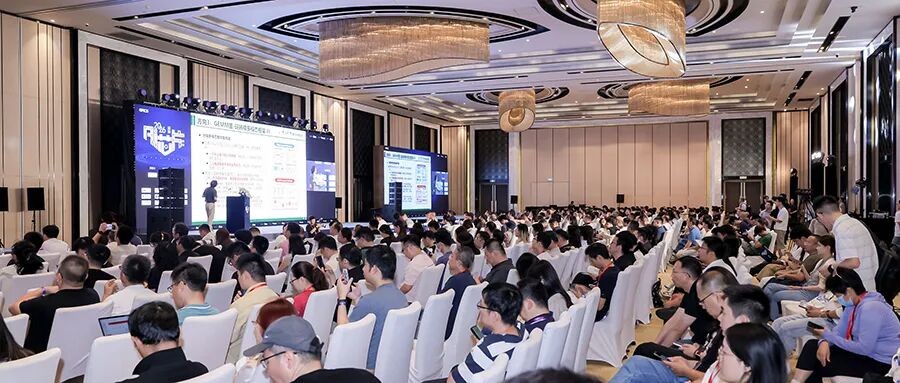
Reported by Chipsn on September 21, the 2026 Global AI Chip Summit concluded successfully in Shanghai recently.
Hosted by Aidigi, organized by its subsidiary Zhixingxing and co-organized by Chipsn, the conference took "Exploring the Path of Chips, Gathering Strength to Go Far" as its theme, providing a full-perspective insight into the key link of AI computing power from TOPS to Token.
Over two full days, more than 60 heavyweight guests delivered a wealth of content on technological innovation, practical implementation and industrial trends at 1 opening ceremony, 3 forums and 5 closed-door seminars. Many speakers also previewed heavy new products at the conference.
The conference focused on the cutting-edge of AI chips, covering key topics such as architecture innovation, 3D stacking, super nodes, KV Cache, new-type storage, heterogeneous mixed training and inference of Token factories, large model inference, agent inference, and embodied intelligence inference. Professional audiences from more than 100 AI chip ecological enterprises came to the site for communication.
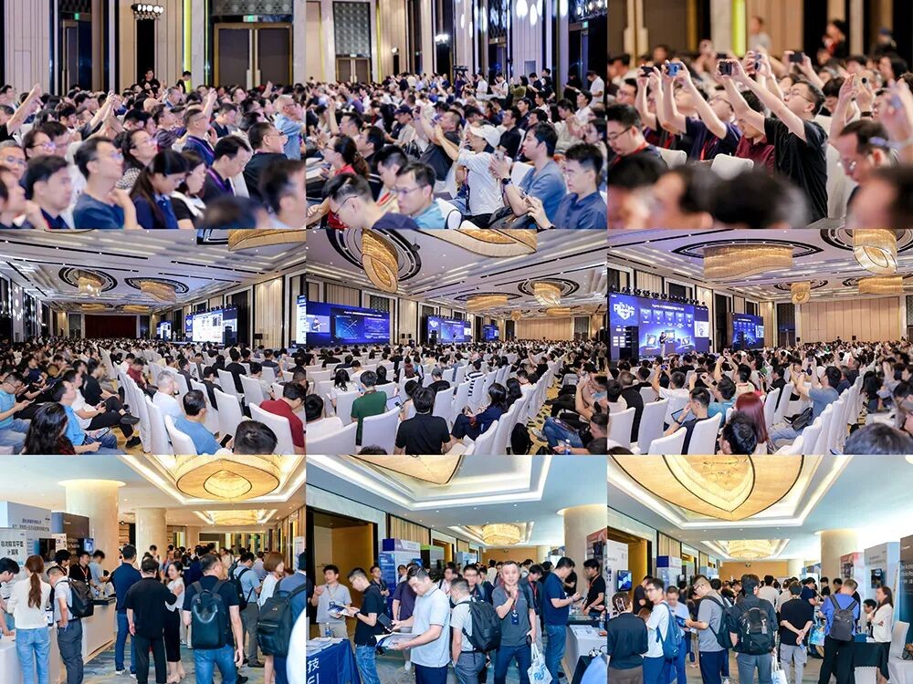
In the exhibition area, enterprises including Quarchip, Nuclei System Technology, Imagination, DINGTEC, Moresilicon, Asterfusion, Qixin Chenguang, KEHUA DATA, Bolun Zhihui, Silicore Technology, Advanced Compilation, Henghan Microelectronics and Yanrong Technology brought the latest technical product solutions for display.
"Nine years ago, we held the first Global AI Chip Summit in Shanghai. Over the past nine years, the Global AI Chip Summit has been held in Beijing, Shenzhen and Shanghai," said Gong Lunchang, Co-founder and CEO of Aidigi, in his address, "This is a microcosm of our continuous attention to the entire AI field."
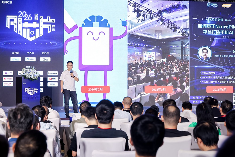
Gong Lunchang, Co-founder and CEO of Aidigi
We have sorted out and summarized the sharing content of 30 guests at the opening ceremony and 3 peak forums (Large Model AI Chip, Agent Inference Chip, Embodied Intelligent Chip), the key points are as follows:
I. Cloud AI Chip Competition! High-efficiency Computing Power Calls for New Architecture, CPU Returns to the Focus of the Agent Era
With the outbreak of agents, the global AI chip industrial pattern continues to evolve. Leading model manufacturers are deeply involved in chip architecture customization. Almost every cloud computing giant is self-developing AI chips, domestic AI acceleration cards continue to be released, and the focus of computing power operation has shifted from seizing high-end computing power at all costs to refined operation centered on token cost and computing power utilization.
How to improve the training and inference efficiency of large models through technological innovation? Why does the agent era call for a "hexagonal" CPU? What are the new solutions to break through the bottlenecks of computing power, memory and network? How can large models help improve chip design efficiency? 5 speakers shared their achievements and insights at the opening ceremony with witty remarks.
1. Wang Zhongfeng from Sun Yat-sen University: Make Full Use of AI Chip Computing Power and Let Large Models Participate in Chip Design
Wang Zhongfeng, Dean of the School of Integrated Circuits of Sun Yat-sen University and IEEE/AAIA Fellow, shared the design challenges and evolution direction of AI chips in the era of large models. At present, how to convert the peak hardware computing power into effective computing power for model deployment has become a key issue. To achieve efficient deployment, his team reduces data overhead through technological innovation of compression and quantization, and improves inference efficiency based on software and hardware collaboration.
In terms of model-driven chip design, Wang Zhongfeng's team solves the challenges of operator adaptation, storage scheduling and sparse utilization through the design of visual Mamba high-efficiency accelerator, ultra-low BitLLM inference accelerator and multi-level sparse Transformer accelerator; for large model-assisted chip design automation, innovations such as performance-aware GEMM Verilog generation design and GEMM graph-code conversion multi-modal framework are proposed.
Wang Zhongfeng believes that the evolution direction of improving AI effective computing power will be the collaborative innovation of model, hardware and system design, including exploring lower bit model compression and precision adaptation, jointly optimizing operator fusion and data reuse, and using deployment feedback to drive model iteration.
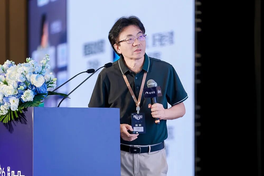
Wang Zhongfeng, Dean of the School of Integrated Circuits of Sun Yat-sen University and IEEE/AAIA Fellow
2. Gao Yu from Intel: In the Agent Era, CPU Returns to the Center Stage
Gao Yu, General Manager of Technology Department of Intel China, said that the outbreak of agents drives the demand for CPU, memory, SSD and privacy, making CPU bid farewell to the past role of "assisting" GPU and return to the center of the AI computing power system.
The operation of an agent is a cyclic process, and its main thread mainly runs on the CPU. The CPU is responsible for context processing, calling large models, permission checking, tool calling and result processing.
A CPU suitable for agents cannot only pursue single-point performance, but become a "hexagonal warrior", with higher sandbox concurrency, IPC and frequency, larger memory capacity, as well as hardware acceleration and security capabilities.
Gao Yu previewed that Intel will showcase the high-density CPU cabinet design with 128 or 192 Granite Rapids processors at the Intel Connection conference two days later, and a single cabinet can carry 50,000 Agents running concurrently.
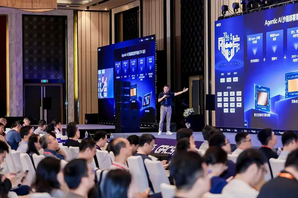
Gao Yu, General Manager of Technology Department of Intel China
3. Hu Yang from Tsinghua University: Improve Token Economy Through Wafer-level Collaborative Design
Hu Yang, Associate Professor of the School of Integrated Circuits of Tsinghua University, pointed out that the value of AI infrastructure should not only be measured by the peak computing power of a single chip, but also consider the effective Token output and the full life cycle investment of equipment, network, power supply and cooling. His team carried out full-system collaborative design from computing chiplets, wafer-level chips to clusters around Token economy.
Aiming at the three major bottlenecks of communication, power consumption and integration density, the team optimized the ratio of computing, storage and communication resources according to task requirements, area and power consumption constraints. At the system level, high-bandwidth communication is transferred into the wafer, and the interconnection, power supply and cooling inside and outside the wafer are jointly designed to reduce communication waiting and peripheral equipment investment.
The report introduced the research progress of model deployment, expert layout and cluster networking. Through collaborative optimization of Token mapping and expert load balancing, the MoE inference scheme achieves 1.84 times the throughput of the control scheme on a single chiplet under the constraint of 4ms Token output interval. The power cost of the inter-wafer networking scheme in the evaluated configuration is 46% lower than the baseline. Relevant studies have explored the wafer-level economy from two aspects: improving effective output and reducing system input.
Hu Yang emphasized that performance benefits need to be evaluated together with manufacturing and operation costs. The team has incorporated thermal warpage, manufacturing and assembly yield, fault tolerance and heat dissipation constraints into the design, and jointly developed a domestic wafer-level chip prototype with Qingmicro Intelligence, forming the capabilities of large-size silicon substrate design PDK, chiplet integration and system verification. It also jointly built software infrastructure with Qingmicro Intelligence and Pujiang Laboratory.
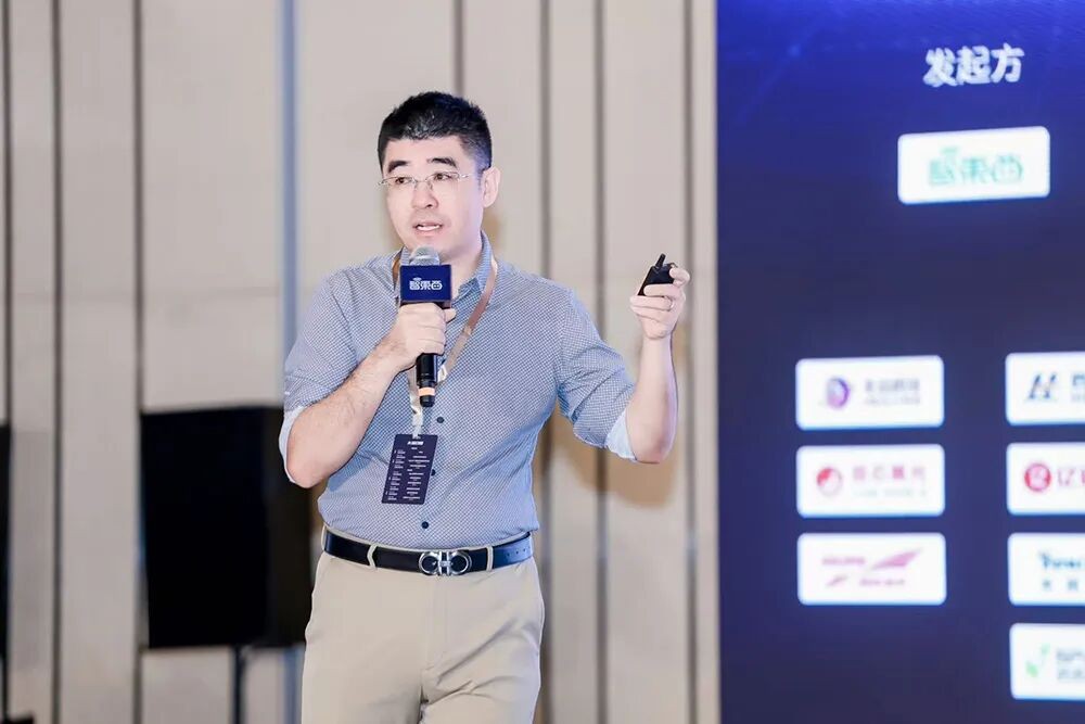
Hu Yang, Associate Professor of the School of Integrated Circuits of Tsinghua University
4. Xin Xiaoxu from Morethan Semiconductor: M50 Has Been Adopted in More Than 150 Products, and Phased Achievements Have Been Made in 3D CIM Architecture
According to Xin Xiaoxu, Co-founder and Vice President of Products of Morethan Semiconductor, in response to the two major challenges of AI chips to improve computing power and memory access, Morethan Semiconductor, as a pioneer of compute-in-memory, has iterated along the SRAM-based compute-in-memory route in the past six years, successfully bringing the compute-in-memory architecture from the academic circle to the industry. Its flagship product M50 has been mass-produced for half a year, with more than 150 product adoptions, forming a commercial closed loop.
Aiming at the problems of limited computing power and poor heat dissipation of the mainstream 3D stacking technology in the industry, Morethan Semiconductor has self-developed 3D CIM architecture, which doubles the computing power under the same area, and significantly optimizes power consumption and heat dissipation pressure. Xin Xiaoxu said that Morethan Semiconductor will carry out technological evolution around the new demands of end-side AI for computing power, energy efficiency and storage bandwidth, and accelerate the industrialization exploration of 3D CIM architecture chips.
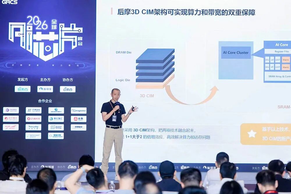
Xin Xiaoxu, Co-founder and Vice President of Products of Morethan Semiconductor
5. Wang Xiaoyang from Quarchip: Future AI Chips May Adopt New Architecture of Custom Memory (HBM+HBF) + Standard Interconnection
In the view of Wang Xiaoyang, Co-founder and Vice President of Quarchip, AI chip design is gradually moving towards customization, heterogeneity and specialization, bringing new opportunities for memory architecture innovation. HBM Base Die customization and HBF layered storage have become new trends.
HBM memory has evolved from a standard single product to a small subsystem, which needs to be deeply customized for different workloads. HBF adopts NAND Flash customized stacking to achieve HBM-level bandwidth but with an order of magnitude higher capacity. In the future, AI chips may adopt a hybrid architecture of NAND Flash (HBF) + HBM, leaving latency-sensitive data such as KV Cache and Attention in HBM, and offloading predictable expert weights to HBF.
Quarchip has full-stack memory and interface IP, with deep accumulation in interfaces such as UCIe, HBM, LPDDR, ONFI/NAND, and can provide interface base technology for custom memory + standard interconnection architecture. At present, the standard package 32G of Quarchip M2 UCIe: interface base has completed silicon verification, and its Chiplet product ML100 IO Die can realize the decoupling of HBM and xPU, which has been taped out and delivered to customers.
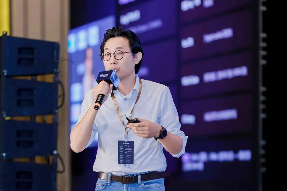
Wang Xiaoyang, Co-founder and Vice President of Quarchip
II. Matrix Partners Roundtable: The Democratization of AI and the Future of End-side Analog Computing
The Matrix Partners roundtable was hosted by Tong Ti, Partner of Matrix Partners China. Four guests, Yang Zheyu, Founder of Seevision, Sun Zhong, Chief Scientist of AnenaIC, Zhan Yi, Founder of Circore, and Chen Zhongming, Chief AI System Engineer of Morethan Semiconductor, shared around the theme of "The Democratization of AI and the Future of End-side Analog Computing".
Tong Ti, Partner of Matrix Partners China, outlined two key points for this roundtable: First, the democratization of AI. AI services for the wealthy is a phased intermediate process, and there will definitely be a large number of products and services for ordinary people in the future; second, on the end side, traditional GPUs and digital NPUs are "old architectures", and more new technologies are needed to solve current problems in the future.
Computing chip companies have water, but they also need supporting pipes. The pipes here represent the model specification capabilities that the chip can support. Tong Ti believes that having core computing capabilities is a prerequisite for enterprises, and the selection of storage architecture is determined according to different application scenarios, based on the parameter scale of the corresponding model and system requirements.
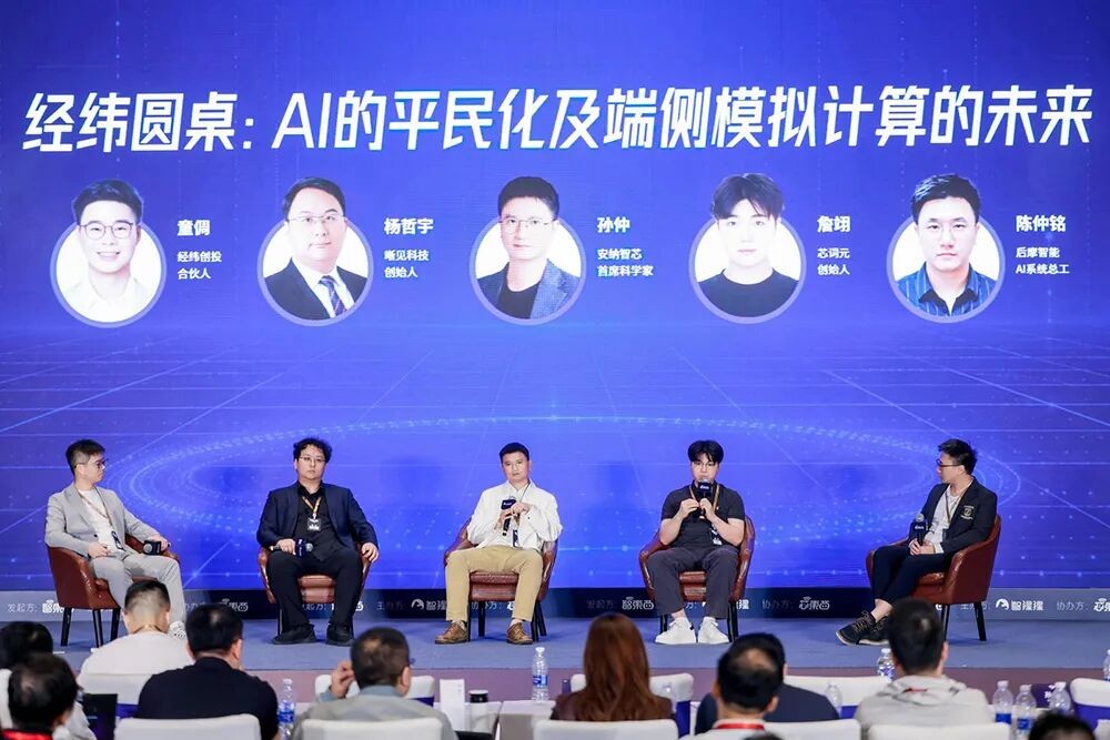
From left to right: Tong Ti, Partner of Matrix Partners China, Yang Zheyu, Founder of Seevision, Sun Zhong, Chief Scientist of AnenaIC, Zhan Yi, Founder of Circore, Chen Zhongming, Chief AI System Engineer of Morethan Semiconductor
1. Yang Zheyu from Seevision: The Tianmou Chip Achievement Was Featured on the Cover of Nature, Realizing Physical AGI
Yang Zheyu, Founder of Seevision, said that end-side intelligence or the broader category of Physical AGI is the next opportunity comparable to AI Coding, and Seevision aims to give AI eyes to see the world. Its 3D IC chip Tianmou, which integrates sensing, storage, computing and transmission, is a chip that can directly output tokens, and the relevant paper was published on the cover of the top international journal Nature.
The structure of Tianmou chip is based on 3D stacking technology, stacking high-density storage arrays and computing units under the photosensitive array, reducing the conversion frequency of ADC through analog computing, and its power