This type of seemingly insignificant material is becoming the new bottleneck for AI optical modules.
Driven by the skyrocketing demand for AI large model training and inference, 800G and even 1.6T high-speed optical modules are hitting a critical node of large-scale volume ramp-up. However, just like the plots that have unfolded many times in the semiconductor industry chain in the past, when the entire optical industry chain is focusing on core components such as DSP chips and EML lasers, a seemingly marginal, inconspicuous niche material has quietly evolved into a new bottleneck restricting production capacity delivery — Aluminum Nitride (AlN) thin-film substrate.
Undercurrents in this industry chain have started to send signals in the capital market and the industrial sector.
On September 17, Zhongci Electronics explicitly stated in its latest institutional survey that as a key packaging material for low-cost non-hermetic packaging solutions, aluminum nitride thin-film substrates are currently in a state of supply falling short of demand. More notably, this is not an isolated signal from a Chinese company. Japan's leading high-purity aluminum nitride powder manufacturer Tokuyama has just announced a production capacity expansion of about 30%; another globally important electronic ceramics manufacturer MARUWA is also expanding its production capacity for next-generation high-speed communications.
An expansion chain that extends all the way upstream from 1.6T optical modules to ceramic substrates and even aluminum nitride powder is gradually taking shape.
Why Aluminum Nitride?
The Inevitable Choice Under the "Thermal Pressure" of Optical Modules
The first challenge comes from an increasingly intractable problem: heat.
Driven by the demand for AI large model training and inference, data center networks are rapidly upgrading from 400G to 800G and 1.6T.
LightCounting predicts this year that the shipment volume of 800G optical modules will more than double again in 2026; the shipment of 1.6T will rapidly rise from a small scale in 2025 to the order of tens of millions of ports. In 2025, the shipment volume of 800G PAM4 chip sets has nearly tripled. TrendForce estimates that the global AI optical transceiver module market will reach approximately 26 billion U.S. dollars in 2026, with a year-on-year increase of over 57%; the shipment proportion of high-speed optical modules of 800G and above will also continue to rise rapidly.
The upgrade from 400G to 800G and 1.6T means higher single-channel rate, more densely arranged optoelectronic devices, more complex signal integrity design, and more lasers, driver chips and DSPs compressed into a limited space.
At the same time, the power consumption of optical modules continues to rise. In the 1.6T era, the typical power consumption of high-speed pluggable optical modules has reached the 20-30W range, and some OSFP systems even need to reserve capacity for thermal design above 30W.
The laser itself is a device highly sensitive to temperature. If the generated heat cannot be dissipated in time, it will not only cause wavelength drift and output power variation, but also accelerate the performance degradation of the device and affect long-term reliability.
Therefore, a previously inconspicuous "gasket" is becoming increasingly important. It is the aluminum nitride chip submount, namely AlN Submount.
Kyocera explicitly pointed out in its optical communication product introduction that as optical communication modules continue to become smaller and more highly integrated, aluminum nitride is becoming an important material for laser diode chip submounts.
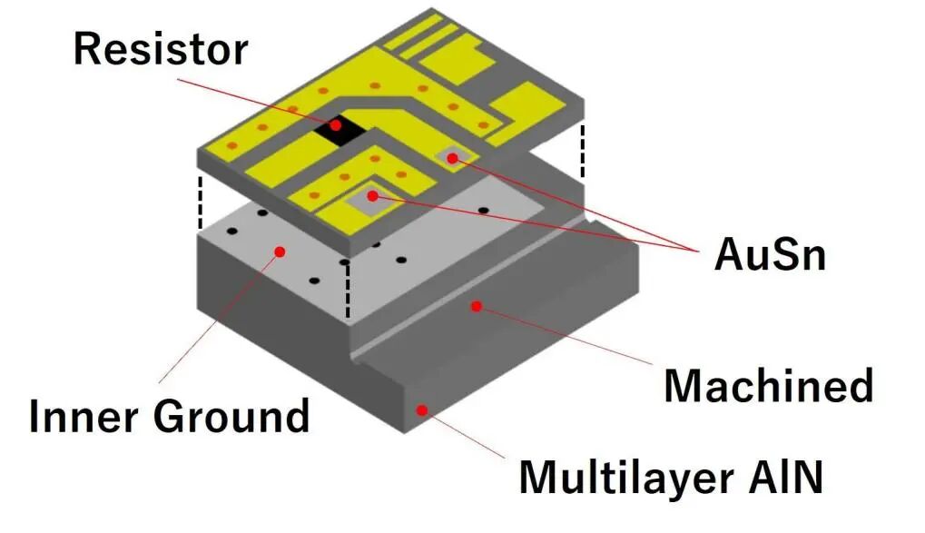
The so-called aluminum nitride thin-film substrate is essentially made of aluminum nitride ceramic as the base material, which goes through precision grinding and polishing, and then forms metal circuits, pads and chip interconnection structures on the ceramic surface through thin-film processes such as sputtering, photolithography, etching and electroplating, and finally becomes the carrying platform for optoelectronic chips such as lasers.
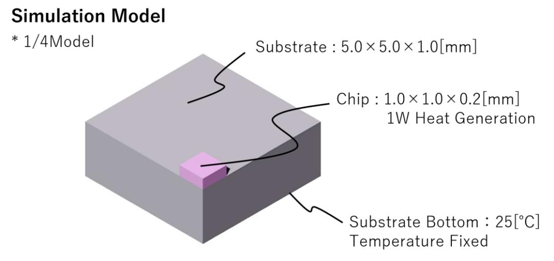
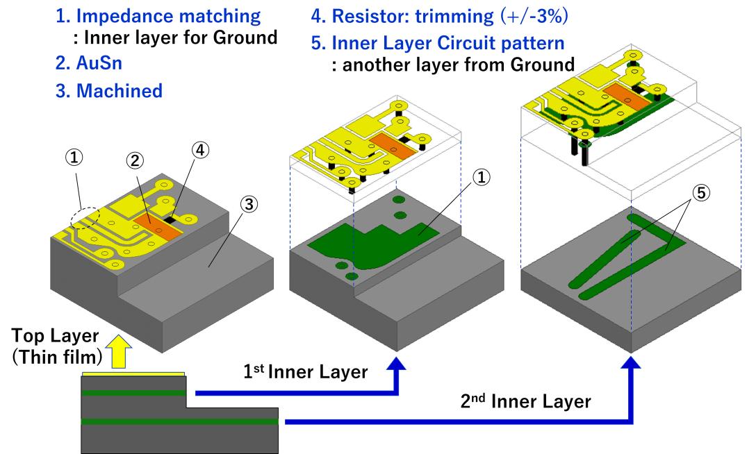
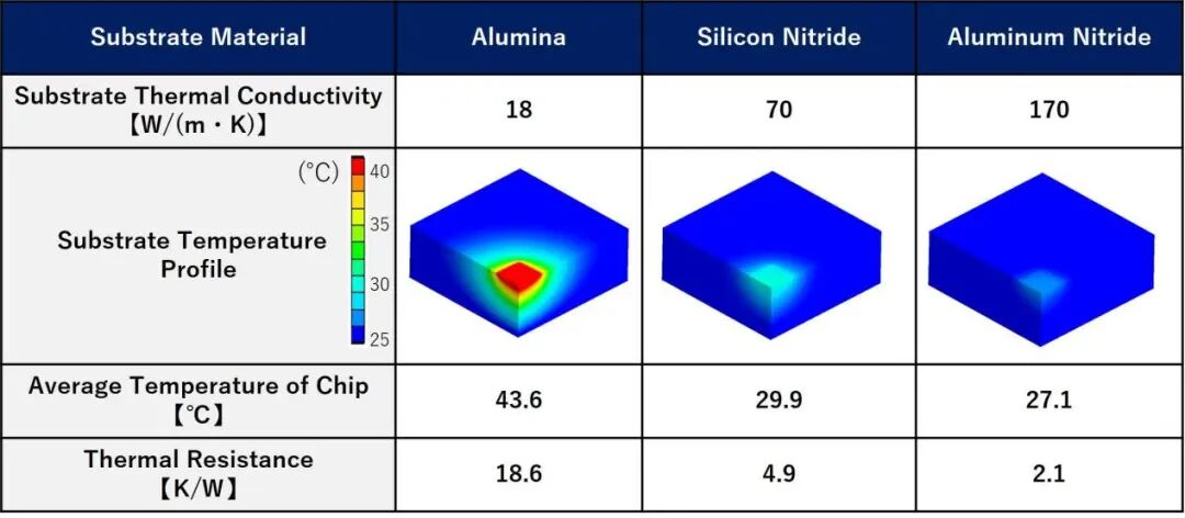
Comparison of thermal conductivity simulation results of ceramic materials (Source: Kyocera)
Its biggest advantage can be summed up in four words: extremely high thermal conductivity.
Public material data from MARUWA shows that the thermal conductivity of its different grades of aluminum nitride ceramic substrates at 25°C can reach 180-230W/(m·K); in contrast, ordinary alumina ceramics only have a thermal conductivity of about 24W/(m·K). The maximum difference in thermal conductivity between the two can be nearly an order of magnitude.
(Source: Kyocera)
But the value of aluminum nitride is not limited to thermal conduction. It also has good electrical insulation, and its thermal expansion coefficient is about 4.6×10^-6/K, which is very close to that of semiconductor materials such as silicon. Therefore, when the device is repeatedly heated and cooled, the mechanical stress generated by thermal expansion and contraction of different materials is easier to control. This makes it very suitable for placement under optical chips. The heat generated by the laser chip can be quickly transferred to the bottom heat dissipation structure through aluminum nitride; at the same time, the ceramic realizes electrical insulation, mechanical support and high-frequency circuit wiring.
Another important change comes from the optical module packaging route of data centers itself.
Traditional telecom-grade optical devices often use hermetic ceramic shells or metal shells for packaging to prevent the intrusion of moisture and pollutants. This solution has high reliability, but has a complex structure and high cost. In contrast, the internal environment of data centers is relatively controllable, and AI clusters have an extremely large demand for high-speed optical modules, so cost, volume and power consumption are more sensitive indicators.
As a result, high-speed data center optical modules are increasingly adopting low-cost non-hermetic packaging solutions. This has actually changed the value distribution of ceramic materials in optical modules. It is a circuit board, an insulating layer, and a heat dissipation channel at the same time. As optical modules become smaller and hotter, these capabilities are becoming irreplaceable at the same time.
Two Japanese Manufacturers Have Started Capacity Expansion
As the absolute leader in the global aluminum nitride powder field, Japan's Tokuyama controls the core reduction nitriding process for high-purity, ultra-fine aluminum nitride powder. Tokuyama is located further upstream than ceramic substrates. Before substrates, there is powder. High-quality aluminum nitride powder ultimately determines the purity, density and thermal conductivity of the ceramic after sintering. If the powder supply cannot increase synchronously, it will be difficult for substrate manufacturers to actually release their production capacity even if they expand production.
Tokuyama says it has the world's largest AlN powder production capacity and claims to lead the global market share. On September 10, it announced that it will build a second aluminum nitride powder production base to increase its aluminum nitride powder capacity by about 30%. The new production line is located in Yanai City, Yamaguchi Prefecture, Japan, and is scheduled to start commercial operation in April 2028. The project is also included in the supply guarantee plan under Japan's Economic Security Promotion Act. Tokuyama's reason for the expansion is that the increase in AI-related investment and the continuous improvement of semiconductor performance are driving the medium and long-term growth of demand for aluminum nitride, and the company needs to enhance its supply capacity.
The second signal comes from MARUWA. MARUWA is one of the world's important high-end electronic ceramics manufacturers. It has been producing aluminum nitride substrates since 1985. Its current products cover a thermal conductivity range of 170-230W/(m·K), and it has integrated processing capabilities for materials, sintering, thin films, metallization and other links.
In its business plan announced this year, MARUWA expects its information and communication business to grow by 23% year-on-year in FY2026, and stated that in order to cope with the substantial increase in demand for next-generation high-speed communication products, it will expand production capacity through the new plant of its Seto Factory. At present, the second plant of the Seto Factory for next-generation communications will be put into operation in FY2026, and the third expanded plant has also started construction.
On the one hand, the aluminum nitride powder leader Tokuyama is expanding production, and on the other hand, MARUWA, which has aluminum nitride substrate capacity, is expanding its factories for next-generation high-speed communications. Both upstream and downstream are increasing capital expenditures at the same time. This further shows that the demand for ceramic materials brought by high-speed optical communication is no longer just a short-term order fluctuation.
At this year's CIOE 2026, the high-speed optical communication packaging products displayed by Kyocera include aluminum nitride chip submounts, multi-layer aluminum nitride substrates, high-speed BOX shells, OCS ceramic shells, LTCC multi-layer substrates, etc. These solutions cover 800G, 1.6T and higher-rate optical communication modules. Major global electronic ceramics enterprises are increasing investment in the same direction.
The problem is that aluminum nitride is not an ordinary ceramic that can be produced in large quantities quickly just by investing in building factories. The real difficulty is turning a pile of powder into a ceramic substrate that has high thermal conductivity, high insulation, high reliability and a sufficiently precise surface at the same time.
The first point is powder purity. The thermal conductivity of aluminum nitride is very sensitive to oxygen impurities. Oxygen impurities in the lattice will significantly increase phonon scattering, which is an important factor limiting the thermal conductivity of aluminum nitride ceramics. In other words, powder purity, oxygen content and the subsequent sintering process will all directly affect whether the final product can meet high-end packaging requirements.
The second point is sintering. Aluminum nitride is a strong covalent bond material with weak atomic diffusion ability, and it is very difficult to sinter to full density. Actual manufacturing usually requires a temperature of 1700°C or higher, and sintering aids, atmosphere and temperature curves are used to control the grain and impurity distribution inside the ceramic.
After that, there are grinding, polishing, laser processing and metallization processes.
Especially at the stage of thin-film substrates used in optical modules, what enterprises sell is no longer just "a piece of ceramic". It is also necessary to fabricate fine metal circuits, pads, AuSn welding layers and other structures on its surface, and control flatness, surface roughness, metal adhesion and high-frequency characteristics. To a certain extent, it has evolved from traditional ceramic manufacturing to a precision processing industry with characteristics of semiconductor manufacturing.
This precisely explains why the capacity expansion of aluminum nitride is not fast. From high-purity powder, to tape casting and sintering, to grinding and polishing, thin-film metallization, precision processing and final customer certification, every step will affect the yield.
What is truly scarce in this type of industry is not "nitrogen" and "aluminum". It is the process capability and effective production capacity to stably manufacture high-quality aluminum nitride substrates.
Domestic Manufacturers Are Accelerating Penetration
From high-purity powder to precision sintering, and then to thin-film metallization wiring, aluminum nitride thin-film substrates have extremely high technical barriers. Facing the increasingly severe capacity bottleneck and huge domestic substitution space, local Chinese enterprises are also rapidly deploying to achieve breakthroughs in this niche track.
Zhongci Electronics explicitly stated in its latest institutional survey on September 17 that its revenue from electronic ceramic materials and components business in the first half of the year increased by 70.16% year-on-year, and the growth momentum mainly came from AI computing power and high-speed optical communications; orders for ceramic shells and ceramic substrates for optical modules have increased significantly. As early as May and June this year, the company had publicly stated on many occasions that aluminum nitride thin-film substrates were in short supply, so at least from Zhongci's own operating conditions, this supply tension has lasted for several months.
Zhongci Electronics said its aluminum nitride thin-film substrates have achieved mass supply, and its optical communication ceramic shells and substrates business is at the global leading level. Its optical communication ceramic shells and substrates cover from 2.5G all the way to 800G, 1.6T and 3.2T, and the 1.6Tbps products have been supplied in batches. In the first half of this year, the company's revenue from electronic ceramic materials and components reached 1.651 billion yuan, a year-on-year increase of 70.16%. This category includes products such as aluminum nitride substrates and ceramic shells.
Sinocera Materials is trying to open up the full chain of "powder - ceramic - metallization". Its subsidiary Sinocera Saichuang has reserved technology for optical module ceramic substrates, among which products related to TEC cooling plates have been sold to some customers in small batches, and other customers are still in the verification process; the second-phase plant has been completed and is gradually ramping up production. At the same time, the company is also jointly developing multi-layer ceramic substrates for AI data centers with customers.
Sunlord Electronics also lists aluminum nitride ceramic substrates and HTCC ceramic shells as important deployment directions for AI optical communications. Sunlord Electronics pointed out in its 2026 semi-annual report that the evolution from 800G to 1.6T and CPO is increasing the power and heat flux density of high-speed optical engines, which in turn drives the demand growth of precision ceramic products such as aluminum nitride ceramic substrates and HTCC ceramic shells. The company has deployed high-thermal-conductivity aluminum nitride multi-layer ceramic substrates and ceramic products related to optical module packaging.
In addition, there is Fujian Huaqing Electronic. Compared with the listed companies above, Huaqing focuses more on aluminum nitride materials itself. It is one of the earlier enterprises in China to realize large-scale production of aluminum nitride ceramic substrates. Its public products cover multiple links such as aluminum nitride powder, ceramic substrates and copper-clad ceramics, and lists AI computing power, 800G/1.6T optical modules and CPO as important application directions.
Another notable new player is Focuslight Technologies. In August this year, the company announced an investment of about 344 million yuan to build the "Industrialization Project of High-Performance Substrate Materials for High-Speed Optical Communication Lasers". The project covers aluminum nitride ceramic substrates, thin-film metallization, photolithography patterning, AuSn thin-film deposition and eutectic bonding. The target product is exactly the pre-deposited AuSn aluminum nitride substrate used in the high-speed optical communication field, and its downstream applications directly point to silicon photonic CW light sources and NPO, CPO external lasers.
It can be seen that China's aluminum nitride industry chain is gradually extending from the past applications focused on basic materials and power semiconductors to the more precise and high value-added AI optical communication market.
Conclusion
The evolution of hardware systems often follows the "barrel theory", and the short board of any marginal link may slow down the overall delivery progress. With the accelerated transformation of 800G/1.6T optical modules to low-cost non-hermetic packaging, this inconspicuous "small material" is becoming a non-negligible key bottleneck in the construction of AI infrastructure, and also opens up a highly imaginative growth space for local players with full-industry-chain independent controllability capabilities.