Why is everyone eyeing 3D DRAM?
In recent months, a distinct trend has emerged in the field of artificial intelligence inference accelerators. Multiple companies have hinted in their roadmaps that they will stack DRAM together with computing capabilities.
Qualcomm has released HBC (High Bandwidth Computing) technology. Later at the Hot Chips conference, Cerebras stated that the CS-6 chip will stack DRAM chips on top of its computing chip. Samsung has spared no effort to promote its zHBM technology and regards it as the ultimate goal. There are rumors that the Groq LP40 is also considering adopting stacked DRAM. In addition, d-Matrix showcased its second-generation accelerator Raptor at the Deep Dive Conference, which also uses stacked DRAM, and announced a partnership with NVIDIA.
In this article, I will explain the rationality of this trend. I will dive into three specific reasons.
1. 3D DRAM enables the highest-performance architecture
2. 3D DRAM can reduce power consumption to below 0.1 pJ/bit, freeing up more power budget for computing and network communication.
3. Unlike HBM, access to 3D DRAM can be deterministic just like SRAM.
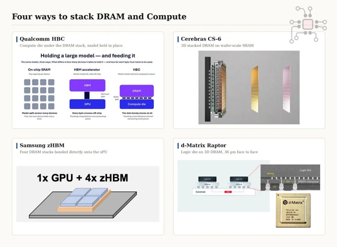
3D DRAM Enables the Optimal, Highest-Performance Architecture
The most exciting part of this year's NVIDIA GTC conference was the fireside chat between two giants in the tech industry — Bill Dally, Chief Scientist of NVIDIA, and Jeff Dean, former Chief Scientist of Google DeepMind. Both of them have made indelible contributions to modern computing. Among the many topics they discussed, one viewpoint kept lingering in their minds — the most energy-efficient and highest-performance way to handle computing is to place data right next to the tensor engine and avoid moving it as much as possible.
"Typically, performing a multiply-add operation on NVFP4 requires 10 femtojoules of energy, while reading these 4 bits of data from HBM4 (which consumes 3-4 picojoules per bit) requires approximately 15 picojoules. This means that reading one NVFP4 value from external memory requires 1000 times more energy than performing a multiply-add operation. However, reading SRAM only requires approximately 10 femtojoules of energy. The key to reducing energy consumption is to avoid data movement." Billy Dally, GTC 2026
This is essentially the architectural concept behind accelerators such as Groq, Cerebras and d-Matrix, where SRAM is located at the same position as the computing units. However, although SRAM is significantly better than DRAM in terms of bandwidth, latency and energy consumption per bit, its capacity will be exhausted quickly. 3D DRAM is the only way to achieve the next leap forward, which can maintain the bandwidth similar to SRAM while increasing the capacity by an order of magnitude.
Similar to SRAM-based architectures, in 3D DRAM, each tensor core can have its own dedicated memory block, with dedicated lines for read and write operations. This capacity and bandwidth belong exclusively to that tensor core, which is different from HBM, where memory is usually treated as a unified pool shared by all tensor cores.
Jeff Dean compared this ideal architecture of adopting stacked DRAM on the computing side to a pinball machine. You open the gate, and the data will fall to the dedicated tensor core like a rolling snowball.
Now, let's take a closer look at the Raptor accelerator exhibited by d-Matrix at the Hot Chips conference. It is the first 3D DRAM accelerator that has publicly disclosed a large amount of detailed information.
Packaging Architecture: Each Raptor package contains 4 chips.
Chiplet Design: Each small chip in this package is a "sandwich" structure, consisting of one computing chip and one stacked DRAM chip.
Computing Layout: Each chip has 256 tensor engines, each of which is allocated 3 dedicated DRAM banks, with dedicated lines for read and write operations.
Interconnection: Each DRAM bank has a 256-bit bus. That means there are 196K data lanes between the computing units and memory units on a single chip. Therefore, each tensor engine has a 768-bit bus connected to its dedicated DRAM.
One Raptor Chiplet = 256 Tensor Cores x 3 banks x 256 bit-bus/bank = 196K data lanes
One Raptor Package =4 chiplets x 196K = ~800K data lanes
In contrast, there are only 8K data lanes between the Blackwell packaged GPU and its 8 HBM3E stacks, and the 8 HBM4 stacks on the Rubin package only have 16K data lanes.
The advantage of increasing the number of lanes by an order of magnitude is that you can run each lane at a lower frequency, around 500-700 MHz, without requiring the bandwidth of more than 11 Gbps per pin as HBM4 does, and the resulting signal integrity/power integrity (SI/PI) and design complexity. Running 196K lanes at such a low frequency has another huge advantage, which we will elaborate on in the next section.
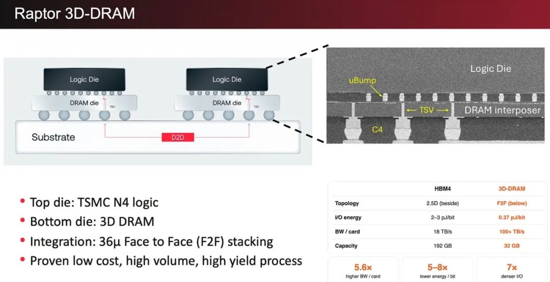
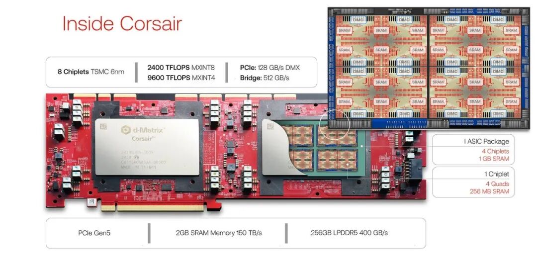
As for the numerical aspects,
1. d-Matrix claims that its performance is based on each pair of chips (8 chip sets), as shown in the figure below. This pair of chips can deliver a memory bandwidth of over 100 TB/s;
2. Compared with the 2GB SRAM of the first-generation Corsair accelerator card, Raptor will be equipped with 32GB of stacked DRAM;
3. At the rack level, 18 computing trays, each equipped with 8 Raptor packages, can provide a total 3D-DRAM capacity of 2.3TB and a memory bandwidth of 7.2 PB/s. In contrast, the NVL rack equipped with 72 Rubin GPUs has an HBM4 bandwidth of 1.6 PB/s;
And this is only the first generation of accelerators based on 3D-DRAM.
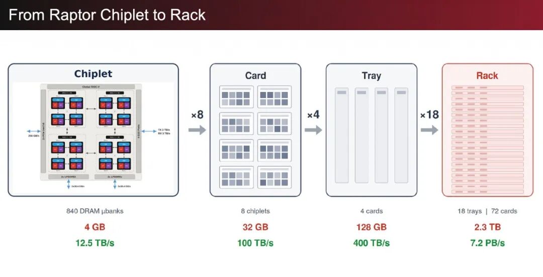
The key point is: multiple companies have elaborated on the advantages of SRAM-based inference accelerators. From the perspective of roadmaps, 3D DRAM is the only way to achieve the next leap forward, which can maintain bandwidth similar to SRAM while increasing capacity.
3D DRAM Can Reduce Power Consumption to < 0.1 pJ/bit
The power consumption perspective is actually very easy to understand.
In HBM, the energy consumption of the DRAM array itself is not the problem. The real problem lies in transmitting data between the memory stack and the computing chip through the interposer. Overcoming such a large capacitance requires high-power drivers, and every segment on the path increases energy consumption — data travels laterally across the HBM substrate to the bumps, down through the interposer, up to the bumps of the computing chip, and then laterally across the computing chip again to the target location. All these steps add up to approximately 2.5 pJ of energy consumption per bit.
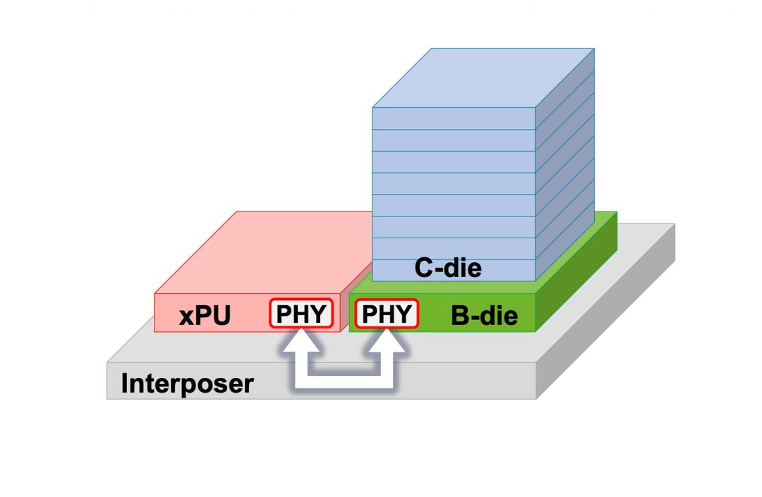
When DRAM is stacked directly on the computing chip, it is easy to imagine how short the transmission distance of data from the DRAM bit cell to the computing execution point is. This completely eliminates the interposer, reducing power consumption to 0.35-0.4 pJ/bit.
To more intuitively understand the difference between 2.5 pJ/bit and 0.4 pJ/bit, we can multiply it by the bandwidth to convert it into watts. Extracting 100 TB/s of data from the HBM stack requires 2000W of power consumption, while extracting it from 3D DRAM requires 296W. Think carefully, the power consumption required to extract 100 TB/s of data from HBM is an order of magnitude higher than that of extracting it from 3D DRAM. The derivation process of these numbers will be introduced in detail below.
HBM power for 100TB/s = 2.5 pJ/bit x 100 TB/s x 8 bits = 2000W
3DD power for 100TB/s = 0.37 pJ/bit x 100 TB/s x 8 bits = 296W
This can also be seen in Samsung's zHBM demonstration. They demonstrated that the power saved by zHBM in a 1200W GPU system can be used to improve computing capabilities.
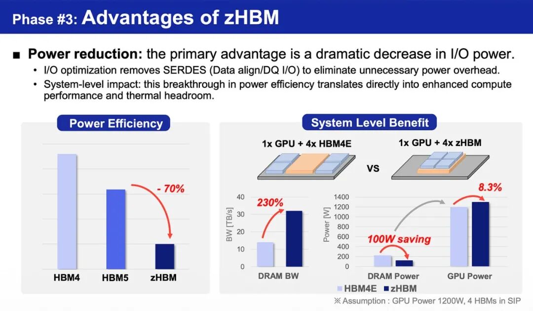
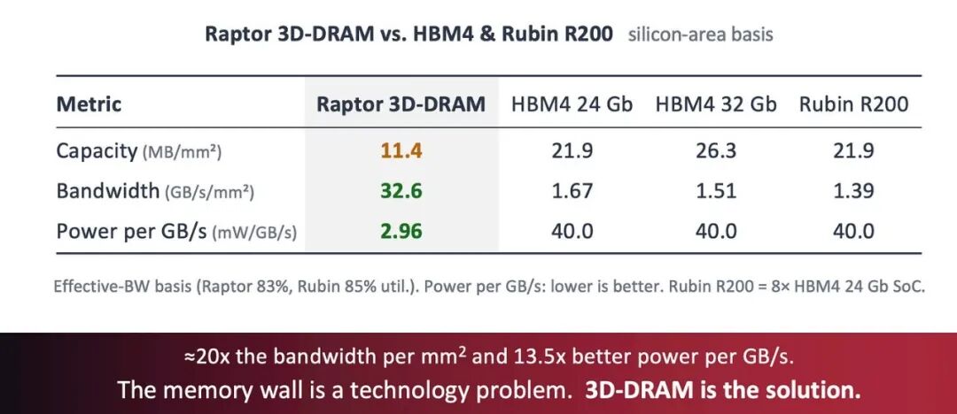
But the key point is that 0.37 pJ/bit is not the lowest value.
Raptor uses micro-bumps with a 36 micrometer pitch to bond the two chips together. Next to such a small pad, a 4-nanometer transistor driver appears very tiny, while the pad, its electrostatic discharge protection, and the wiring leading to the pad constitute a relatively large capacitance by on-chip standards. The situation on the DRAM side is similar.
Hybrid bonding technology significantly reduces chip size. The pin pitch is reduced from 36 micrometers to single-digit micrometers, and the pad size is also reduced accordingly. The wiring distance between the driver in the computing chip and the DRAM is greatly shortened, and the capacitance is also reduced. As a result, energy consumption is further reduced from approximately 0.4 pJ/bit to approximately 0.1 pJ/bit.
The Determinism of 3D DRAM
Okay, the last part of my pitch is — DRAM is notorious for its indeterminism.
HBM, LPDDR and similar memories go through an initialization process called training and calibration at startup. During this process, the HBM PHY on the computing chip runs read-centering and write-centering algorithms. It writes a pre-set pattern to the memory, then reads these patterns, and scans the phase rotator on each lane to find the center of the data eye. I have simplified the description of this process here. If you are interested, I have detailed the specifics in other articles.
Training is just the beginning. After startup, three things can cause DRAM to be in an indeterminate state.
1. Changes in voltage and temperature will cause the optimal eye diagram to drift, so the PHY needs to be recalibrated regularly. This is one of the sources of uncertainty.
2. The refresh process is controlled by temperature. This is a necessary operation, but it directly reduces performance.
3. DRAM is very sensitive to the way data is stored and retrieved. Since HBM is usually regarded as unified memory, the HBM controller will reorder transactions to maximize page hit rate and bank rotation. This makes the latency of any read request indeterminate.
For 3D DRAM, these problems either do not apply or can be easily solved through design.
1. When DRAM is directly bonded to the computing chip, no traditional HBM-style PHY is required due to the extremely short distance. This eliminates the need for training and calibration, and there is no need to consider trace length. The interface between the computing chip and the memory chip is closed through static timing analysis, so this design is sometimes called a PHY-less design.
2. In 3D DRAM, each bank is very shallow, so we can set the refresh rate to a sufficiently high frequency without greatly affecting performance.
3. Each tensor engine has its exclusive paths and pin connections to its bank, and does not share any paths and pins with other tensor engines. Therefore, the controller is very simple and does not need to perform any opportunistic transaction reordering. This makes the access latency deterministic.
The key point is: the deterministic behavior of SRAM has many advantages, and 3D DRAM preserves this feature in a way that HBM cannot. It should be noted that DRAM technology itself is very sensitive to the way data is stored and retrieved. Unlike SRAM, where access patterns do not matter, any type of DRAM, whether HBM or 3D DRAM, requires hardware and software co-design to properly lay out weights and key-value caches to maximize page hit rates.
Conclusion
Common questions include heat dissipation, cooling, warpage, power distribution network (PDN) and yield. These are all reasonable problems and all solvable. Most manufacturers in the industry are already working on solving these problems. HBM5 is expected to adopt hybrid bonding technology, which is poised to enter the mature stage.
In terms of heat dissipation, we may only be able to achieve 4-layer stacking in the short term. 8-layer stacking still has some engineering problems to be solved. The real challenge lies in the power density of the computing chip located under the memory stack. DRAM is very sensitive to heat, and its power consumption is only 0.5 W/mm², so achieving 4-layer stacking may not be a problem. A GPU like Rubin, with a power consumption as high as 1.5 W/mm², may easily achieve 2-layer stacking, but achieving 4-layer stacking may require some engineering design.
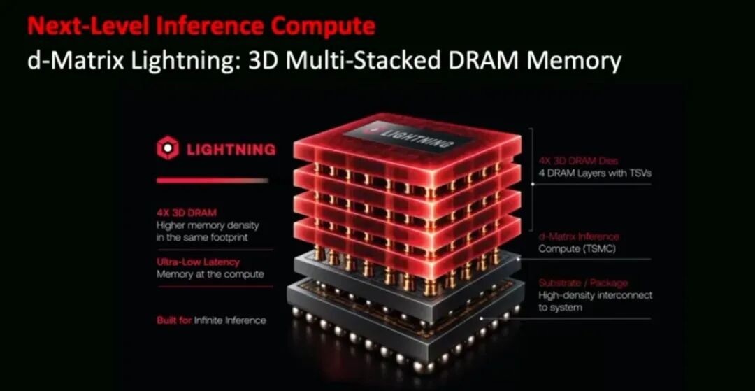
These comments are based on my experience and intuition. The more important point I want to make is that Raptor only uses one layer of DRAM, and its subsequent Lightning accelerator will use four layers of DRAM for a reason. Beyond that, there are many engineering issues to be resolved.
This article is from the We