Memory prices are on fire, and the chip war has broken out again.
"Everyone is scrambling to release and go on sale as early as possible," said a former strategic researcher at a mobile phone manufacturer. "Previously, to avoid competing with the iPhone, the launch of new Android products was generally scheduled in October."
The cutthroat competition between mobile phone manufacturers comes from multiple factors: the consideration of the "Golden Week" and "Double 11" shopping holidays, the need for domestic high-end flagship products to compete head-to-head with the iPhone, and the proven successful formula of the Xiaomi 17 Pro.
"Last year, only Apple and Xiaomi released new products in September. Xiaomi launched a back-screen model, promoted it nonstop, and put it on sale a full month earlier than others. This year, everyone has learned that 'lesson'," the aforementioned researcher said.
All these phenomena, no matter which one you look at, are sufficient to demonstrate the fierce intensity of competition in the smartphone market.
Throughout September, Huawei and Xiaomi released new products on the same day: Huawei launched the new-generation triple-foldable Mate XT2, while Xiaomi rolled out its mid-range foldable flagship Xiaomi 18 Fold. Later, Apple released the iPhone 18 Pro series and its first foldable iPhone Duo.
If brands including OPPO and vivo are counted in, there were nearly 10 new product launches throughout September.
In terms of pricing, high-end flagships are generally priced above 10,000 yuan, with some even reaching 20,000 yuan. At the same time, the underlying chips have also been upgraded to the latest generation, including Huawei's Kirin 9050, Xiaomi Xuanjie O3, Apple A20 Pro, MediaTek Dimensity 9600 Pro, and Qualcomm's 6th-generation Snapdragon 8 Elite series.
It can be said that mobile phone manufacturers, under the pressure of rising memory prices, have joined the 2nm chip competition, and there is a very obvious change in this process: chip makers are collectively going "All in AI".
01
The 2nm Chip Race
In terms of 2nm chips, MediaTek was the first to make relevant announcements back in 2025. MediaTek CEO Richard Lai first teased the product at Computex 2025, and then officially announced in September that the world's first 2nm SoC had entered the tape-out phase.
Leading in tape-out does not mean leading in mass production.
The real 2nm mobile chip war did not officially kick off until this September with the debut of Apple's A20 Pro. "Built with the latest 2nm process technology, the A20 Pro sets a brand new benchmark for mobile computing," Apple emphasized in its official press release.
In terms of mass production and launch time, Apple is the well-deserved first mover of 2nm products, and in terms of customer scale, Apple is bound to get the priority access to 2nm production capacity.
"TSMC's 2nm wafer capacity this year is around 100K, of which Apple takes up about 70K," said Wu Zihao, CEO of Ronghe Semiconductor Consulting who has long tracked TSMC's production capacity. "MediaTek's shipment volume is not large: only a few thousand wafers are enough for the Dimensity 9600 Pro chip, Qualcomm takes up about 10K, plus AMD's nearly 20K, the total adds up to around 100K."
Jeff Pu, senior analyst at Haitong International, previously predicted that Apple will stock up 78 million units of new products including the iPhone Duo in Q3 and Q4 this year. Without considering assembly scrap, the theoretical monthly demand for A20 Pro chips is 13 million units.
Data calculated by well-known testing agency Geekbay shows that the die size of Apple A20 Pro is 98.8mm². Assuming TSMC's 2nm yield rate is 85%, it is estimated that the production capacity demand for the A20 Pro mobile chip is about 25K, and the remaining 45K capacity will be allocated to the 2nm M6 chip.
From the perspective of customer importance, driven by AI demand, Apple has slipped from the position of TSMC's largest customer and been overtaken by NVIDIA. But GPUs do not require the most cutting-edge process, and Apple is still TSMC's core 2nm customer at this stage, which has been the case for many years. The reason why Apple can obtain such priority access not only comes from the deep cooperation relationship established with TSMC in the era of Morris Chang, but also supported by the global sales volume of iPhones.
Although MediaTek has publicly announced its tape-out progress, the demand for 2nm capacity for mobile SoCs is much smaller. Calculated based on a 5K wafer demand, 134.02mm² die size and 85% yield rate, the monthly shipment of Dimensity 9600 Pro is about 2 million units.
It is worth noting that MediaTek is also collaborating with Google to design a 2nm TPU dedicated to AI inference, which is expected to ship by the end of 2027. Once this product enters mass production, it may significantly increase MediaTek's demand for TSMC's 2nm capacity.
Wu Zihao said: "Although Qualcomm, MediaTek and Apple have all launched 2nm chips, MediaTek has relatively few high-end products. Even though it is now the world's largest mobile chip shipper by unit count, most of its products are still mid-to-low end models."
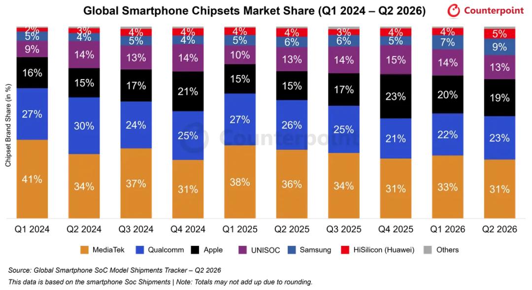
According to tracking data from Counterpoint Research, by the second quarter of 2026, MediaTek's global smartphone chip market share reached 31%, down 2% quarter-on-quarter. In comparison, the figures for Qualcomm and Apple are 23% and 19% respectively.
Another noteworthy topic is that although 2nm is the mainstream process this year, its price has risen just like memory chips. For this reason, Qualcomm announced at its Q2 earnings meeting that it would raise product prices starting from September 1.
Eventually, the price increase of wafer foundry services will be passed on to end mobile phones just like the rise of memory prices. The most intuitive experience for consumers is: mobile phones are getting more expensive.
Price hikes and concentrated product launches also reflect a very harsh reality: stock market competition.
"The overall market performance is not good," said Yu Lei, former vice president of Gionee. "The total sales revenue has not actually declined, what dropped is the shipment volume. This has been the case for several years."
In Yu Lei's view, this price increase is partly related to the rising cost of the supply chain, and partly related to domestic substitution of supply chain components and technological progress. An obvious change is that components including displays, CIS, storage, and radio frequency are gradually realizing domestic substitution, which accelerates the evolution of domestic mobile phones and ultimately leaves Japanese and Korean mobile phone brands at a huge competitive disadvantage.
Another direction of domestic industry advancement is the self-development of mobile phone chips, which we will discuss next.
02
New Forces of Self-developed Chips
2nm chips represented by Qualcomm and MediaTek are one type of solution, while self-developed chips represented by Apple, Huawei and Xiaomi are another.
Apple's path of self-developed chips has fully proved the value of this strategy, and Huawei and Xiaomi have also become practitioners on this path. However, due to foundry restrictions, compared with Apple, the self-development path of Huawei and Xiaomi is much more difficult, but also more valuable to a certain extent.
On September 7, Huawei officially released the Mate XT2 triple-foldable phone, equipped with the Kirin 9050 Pro chip based on the Tao's Law and logic stacking technology. This chip adopts W2W (Wafer to Wafer) technology, which changes the traditional single-layer planar logic unit to double-layer vertical stacking, commonly known as "installing an elevator inside the chip".
Logic stacking is a brand new solution for Huawei's self-developed chips under the restriction of process miniaturization, and it is an important achievement of the implementation of "Tao's Law". Coincidentally, Xiaomi has also adopted the same W2W solution, launching the 6nm Xuanjie O100 chip.
The common point between Huawei and Xiaomi is that advanced packaging has opened the door for chip designers to squeeze out more performance from existing architectures.
However, the differences between the two are also obvious: Huawei's W2W focuses on stacking logic units, while Xiaomi's W2W stacks logic units and storage units. The former mainly solves the bottleneck of physical process miniaturization, while the latter aims to improve the data transmission efficiency bottleneck caused by the memory wall.
Mainstream mobile SoCs from Apple, Qualcomm and MediaTek have all adopted 2nm process this year, while Xiaomi is still using 3nm process. There are multiple factors behind this situation, which we have discussed many times in the past, and one of the key restrictions is the GAA architecture.
For the current 2nm process, both Samsung and TSMC have switched to the GAA architecture, and the design software and wafer foundry services corresponding to this architecture are under strict export controls.
"Xiaomi can only use 3nm process at most," the aforementioned former strategic researcher said.
In fact, from the perspective of scale, even if the current Xuanjie chips adopt 2nm process, it may not be a cost-effective business, the root cause lies in the lack of large-scale shipment volume.
Take Apple as an example: the iPhone product line alone demands hundreds of millions of self-developed chips every year. At present, the shipment volume of Xuanjie O1 has just exceeded 1 million units. We did similar calculations last year, and to achieve real scale benefits, the shipment volume needs to reach 10 million units. From this perspective, domestic self-developed chips are just getting started.
But in fact, the exploration ideas Xiaomi made on the 3nm Xuanjie O3 are far more valuable than simply adopting 2nm process.
According to data disclosed by Xiaomi, the Xuanjie team reconstructed the minimum underlying logic unit Standard Cell of transistors, increasing the number from 480 in O1 to 2400 in the current O3. At the same time, Xuanjie O3 adopts the Channelless channel elimination technology, which cancels the reserved channels for placing BUF units to enhance power supply in traditional SoCs, and moves the BUF units to other modules, achieving a 5% increase in transistor density.
If I have to explain its value: in the past, Moore's Law relied on process iteration from wafer fabs to double the number of transistors per unit area every 18 or 24 months. Now the evolution speed of process technology has slowed down, many people say "Moore's Law is dead" and "Moore's Law no longer works". But Huawei and Xiaomi, under the restriction of process access, have revived Moore's Law with a brand new approach.
China's chip design teams are truly remarkable, and this deserves full recognition.
03
All in on AI
No matter it is Apple's 2nm chips or Xiaomi's 3nm Xuanjie chips, there is a very obvious consensus this year: AI has been integrated into every core IP, and different cores including CPU, GPU and ISP are all participating in sharing AI inference tasks. SoCs are evolving from the old architecture of "a single dedicated NPU handling all AI tasks" to a full-subsystem heterogeneous AI computing power network.
From this perspective, calling it "All in AI" is not an overstatement at all.
Under this computing power network, heavy large model workloads still run on the NPU with priority, while short-latency light AI tasks run directly on CPU-AI or GPU-AI to share fragmented, low-latency small AI tasks and reduce on-chip data transmission overhead.
Data disclosed by the Xuanjie team at the previous Xuanjie O3 briefing shows that the CPU includes two new matrix computing engine units, adopting the SME2 instruction set to provide 3.5TOPS of computing power for processing lightweight AI workloads. The GPU subsystem is equipped with 8-core NX neural acceleration units, with a total computing power of 36TOPS, enabling AI super-resolution and frame interpolation for image rendering inside the GPU.
"Everyone is making attempts in this layout, but the scenarios and practical value of AI on mobile phones are still insufficient at present," a senior chip design expert told Tencent Tech.
"From the perspective of technology evolution trends, embedding AI into GPU is a definite direction, as you can see from NVIDIA's practice. It is reasonable for scenarios that require strong real-time performance such as gaming. Embedding AI into CPU is for small processing tasks, which is largely driven by Apple's practice and ARM's promotion of this capability. These are all definite directions, and the specific implementation schemes can still vary."
According to previously disclosed information, Apple adopts a three-level heterogeneous AI computing architecture: CPU (AMX hardware unit) + GPU (built-in neural network accelerator) + independent NPU. The underlying IP of MediaTek's chips shares the same design logic with Xuanjie O3, adding dedicated AI hardware units to all computing subsystems, which is the most thorough full-module AI implementation among all mobile SoCs this year.
The aforementioned strategic researcher also agreed with the idea of learning from Apple's proven path.
"The AMX unit in Apple's CPU core is mainly used for vector computing and matrix acceleration, running simple algorithms and some RNN models, but it does not support parallel computing. Qualcomm and ARM supported QMX/SME last year, which is basically a copy of Apple's implementation of this function."
In his view, the core of this design concept is to optimize computing "costs". "NPU computing requires the computing core to transmit and schedule tasks, which brings a lot of extra overhead. Therefore, it is more efficient to run some simple calculations locally, inside the core."
Running AI tasks "as close to the data source as possible" not only improves efficiency, but also reduces overhead, which will bring an increase in the overall energy efficiency ratio of the device, and also enables mobile phone manufacturers to explore personalized capabilities based on the AI characteristics of different IPs. "OPPO has made some investments in proactive AI features, and it is possible for them to create differentiated products," the aforementioned strategic researcher said.
The general trend and direction are clear, but the exploration is still in the early stage, and there is no unified implementation roadmap yet.
"The current implementations are not perfect, but AI integration will become more and more extensive in the future. Whether to embed AI units inside the GPU, or to achieve close collaboration between GPU and external NPU, both approaches are viable," the aforementioned chip design expert said.
That means although the "All in AI" trend has a very high profile and the industry has reached a broad consensus, what will really make consumers pay extra for these innovations are reliable, stable, and frequently used scenarios and capabilities that bring tangible value.
This article is from the WeChat official account "Tencent Tech", written by Su Yang, edited by Xu Qingyang, published with authorization from 36Kr.