With the explosive growth of AI inference, has the "unlucky" SanDisk really risen from the ashes like a phoenix?
This round of AI wave has turned NAND flash from a "cyclically oversupplied commodity" into a "strategic resource in short supply". After spinning off and getting rid of the drag of the traditional hard drive business, SanDisk has made a pure bet on NAND and data center SSD, which exactly catches this market outlet.
When AI servers perform inference, process complex Tokens, Prompts, multimodal inputs (videos, images) and generate synthetic data, they need to read and write historical data frequently and repeatedly. The storage configuration of the traditional cloud architecture can no longer meet the demand, and the consumption of NAND flash per node of current AI servers is growing exponentially.
In the stage dominated by training, major manufacturers focus more on competing for computing power; when entering the inference stage, "AI infrastructure = XPU + storage + connectivity", the importance of computing power is weakened, while more attention is paid to the demands of storage and connectivity fields.
How does AI infrastructure affect the overall industry demand for NAND? In fact, AI data centers do not need all NAND products, and the main demand is concentrated on enterprise-level SSDs. In the current era of Agentic AI and large-scale inference, what AI needs most are ultra-large-capacity enterprise-level QLC SSDs and PCIe 5.0/6.0 SSDs with high bandwidth and low latency.
When large downstream CSPs are snapping up enterprise-level SSDs with high premiums and long-term orders, storage manufacturers adjust a large proportion of their original production capacity for mobile phones and PCs to produce AI enterprise-level products. The "squeeze on the supply side" indirectly affects the supply and demand pattern of the entire NAND sector, and drives the overall NAND cycle upward.
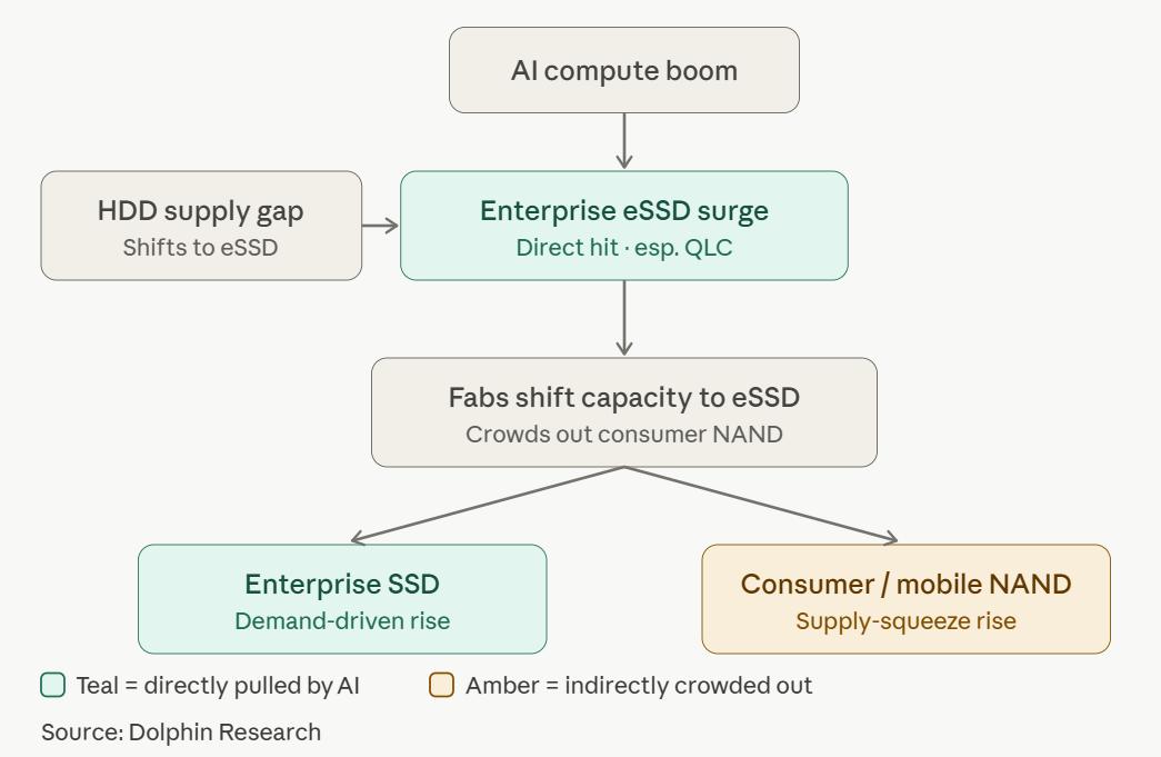
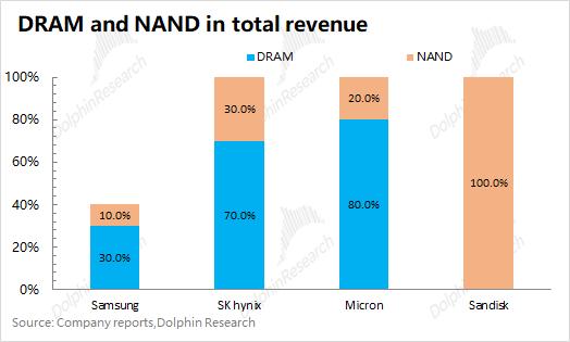
In the NAND market, the main players include Samsung, SK Hynix, Micron, SanDisk, etc., among which SanDisk is the most pure one. The three major original manufacturers still focus on the DRAM and HBM fields. After getting rid of traditional hard drives, SanDisk is fully focused on the NAND flash market and will fully benefit from the current "warming up" of the NAND industry.
For SanDisk, Dolphin will mainly focus on three issues in this article: ① The relationship between SanDisk and Western Digital; ② The cooperation between SanDisk and Kioxia; ③ The industry status of SanDisk's NAND technology. The subsequent performance and valuation pricing of SanDisk will be presented in the next article, and you are welcome to continue to follow.
In terms of technical strategy, SanDisk does not "obsess over" the number of layers, but focuses on "lateral scaling" to achieve the highest bit density in the industry; it takes the lead in mass-producing the CBA bonding architecture to improve performance and energy efficiency; and jointly launches the HBF (High Bandwidth Flash) technology for AI inference. Its comprehensive technology is still in the relatively leading first echelon among NAND manufacturers.
In the context of the strong demand for ultra-large-capacity enterprise-level QLC SSD driven by AI large model inference, SanDisk will continue to enjoy the growth dividend brought by AI infrastructure with the stable production capacity guarantee extended to 2034 in cooperation with Kioxia, the high performance elasticity of "pure NAND" and the potential opportunities of HBF.
Detailed Analysis as Below
I. SanDisk and Western Digital: Ten-year Itch, "Separation" Benefits Both Parties
First of all, let's take a look at what kind of company SanDisk is? Although SanDisk has been listed not long ago, it is actually a "veteran" in the storage industry. Founded in 1988, SanDisk is one of the pioneers of flash memory technology, and was acquired by Western Digital for about 16 billion US dollars in 2016.
Due to the obvious differences in growth and development logic between HDD and NAND products, the whole company will be affected by the market's "undervaluation and discount". In October 2023, Western Digital announced plans to spin off its flash memory business into a new listed company established under the name of SanDisk, while Western Digital specializes in the hard drive business, and achieved "separate" listing again in February 2025.
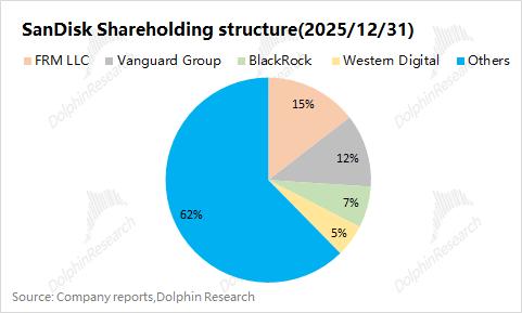
At the time of the spin-off, Western Digital retained 19.9% of SanDisk's shares, and by June 2025, its shareholding had been reduced to about 5%. When Western Digital acquired SanDisk at that time, it borrowed a total of about 18 billion US dollars in M&A loans, and the company has been under the heavy pressure of "high debt" for nearly ten years.
With the continuous rise of SanDisk's stock price, Western Digital also plans to realize the "SanDisk shares" in its hands, so as to reduce the company's debt pressure. The announcement in February 2026 mentioned that Western Digital plans to dispose of all 7.5 million SanDisk shares it holds, which can reduce debts by more than 3 billion US dollars.
Western Digital completed the disposal of 7.5 million shares in two steps:
① 5.82 million shares were disposed of through the method of "debt-to-equity swap and public offering and sale in the secondary market". The specific process is "first borrow a bridge fund -> use the bridge fund to redeem all senior preferred shares -> debt-to-equity swap -> the bank resells them".
② Dispose of the remaining 1.69 million shares through the "share-for-share" method. The specific operation is "exchange SanDisk shares for its own shares, and then cancel the 4.8 million shares obtained from the exchange".
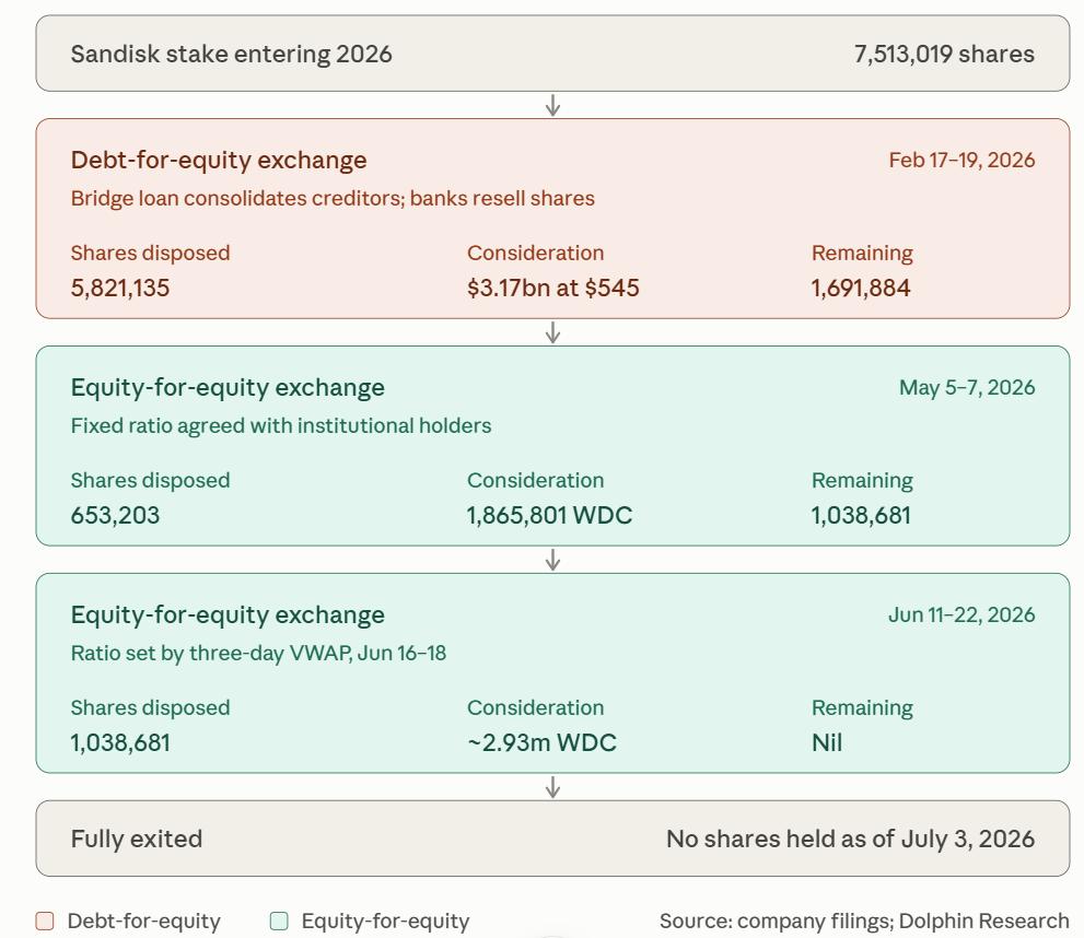
Through the above operations, Western Digital's "spin-off and divestiture" of SanDisk is actually beneficial to both parties: ① Western Digital can reduce debt pressure while focusing more on the HDD field; ② SanDisk has become a completely independent NAND flash and solid-state drive company. The two sides are completely decoupled in equity, and SanDisk has independent dominance without taking into account HDD business anymore.
By the end of 2025, Western Digital is still one of the major shareholders of SanDisk. After Western Digital clears all SanDisk shares, SanDisk will become an independent technology company controlled by Wall Street institutions. Its major shareholders are mainly Fidelity Investments, Vanguard Group, BlackRock and other institutions, and the selling pressure from Western Digital has been digested.
II. SanDisk + Kioxia: 20+ Years of Continuous Cooperation
Compared with manufacturers such as Micron, SanDisk's products are more "single", and the company's revenue all comes from the NAND field. At the beginning, the attention of this AI wave was concentrated in the HBM field, and SanDisk did not benefit at that time. When the storage cycle begins to turn to NAND, SanDisk, which "goes all in NAND", shows more flexible performance.
From the industry perspective, the current NAND industry shipments mainly come from three original manufacturers: Samsung, SK Hynix and Micron, while Kioxia and SanDisk follow the three, accounting for about 15% of the market share roughly.
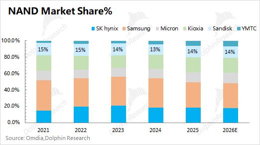
The market shares of SanDisk and Kioxia have been relatively close for a long time. It should be understood that almost all of SanDisk's production capacity comes from Japanese joint ventures, and it shares wafer production capacity equally with Kioxia (roughly at a 4:6 ratio).
Although Toshiba (the predecessor of Kioxia) invented NAND, it lacked the capital and system integration experience for large-scale commercialization; while SanDisk had relevant technology and market channels. Therefore, around 2000, the two sides decided to cooperate to build a wafer fab in Yokkaichi, Japan:
① Joint capital contribution: Purchase semiconductor manufacturing equipment (lithography machines, etc.) to share the risk of heavy assets;
② Shared R&D: Develop the BiCS architecture in the same laboratory (the links before die are jointly developed), and share the technical achievements. For the links after die, the two companies form differentiation through independent R&D;
③ Production capacity allocation: share wafer production capacity equally, each taking about half of the wafers (front-end production capacity) for independent sales.
The cooperative relationship between SanDisk and Kioxia is quite stable. It has experienced the acquisition and independence of SanDisk and the renaming of Toshiba Storage, but the cooperation agreement between the two sides has not been interrupted. After its independence, SanDisk announced in January 2026 that it would extend the joint venture agreement, which was originally due to expire in 2029, to December 31, 2034, ensuring the sustainability of cooperation between the two sides.
The two companies announced on the same day that the BiCS10 engineering samples were sent out in July 2026, with completely consistent specifications —— 332 layers, 1Tb TLC, density over 29 Gb/mm², 59% higher than BiCS8, interface speed 4.8Gb/s (+33%), continuing to use the CBA and OPS technologies introduced in the 8th generation.
At present, SanDisk's NAND wafers are basically from two large bases in Japan: ① Yokkaichi Base, the world's largest flash memory production base, with multiple factories from Fab3 to Fab7; ② Kitakami Base, an emerging incremental base, with K1 and the newly operational K2 factory.
Kioxia announced on August 27 that it has started the site leveling and related preparation work for Fab3 of the Kitakami factory, the factory site is south of Fab2, with the goal of putting into production in fiscal year 2029 for expanding the production of advanced BiCS FLASH.
The two companies announced on the same day that they will invest more than 31 billion US dollars (about 5 trillion yen) in Japan by 2032 (within the extended cooperation agreement), on the premise of obtaining government support. The market expects K3 to account for about 1.8 trillion yen (about 11.3 billion US dollars).
III. NAND Stacking Technology Capability and Economy
When NAND products advance from 2D to 3D, it is no longer just a competition of process, but more importantly, the superposition of layers. The capacity improvement of 3D NAND no longer depends on process scaling, but can be realized by increasing the number of stacked layers, thus jumping out of the "dead end" of process.
The increase of NAND stacking layers can directly bring about the improvement of storage density, which means that the NAND supply can be increased with a small amount of capital expenditure. Therefore, the progress of the number of layers of various manufacturers can also reflect their product capabilities in the NAND field.
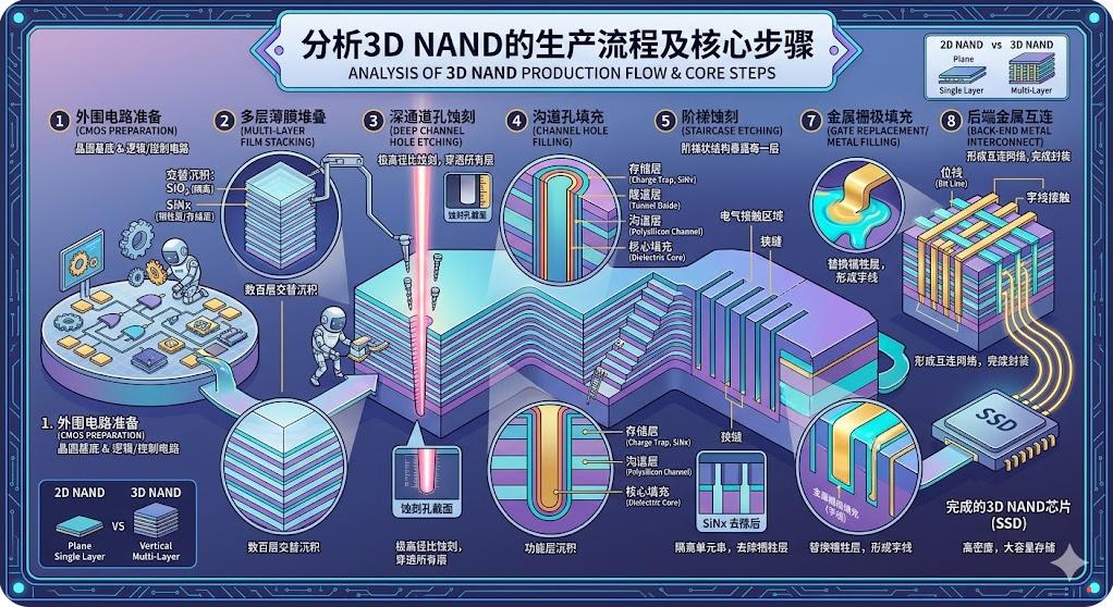
a) Stacking Technology Selection
With the continuous increase of stacking layers, the biggest technical difficulty lies in deep channel hole etching: specifically, in the 200-300 layer film layer, billions of holes with a diameter of tens of nanometers are drilled vertically.
When a single layer is etched to 200-300 layers, it is almost close to the limit. It is like using a fine needle to precisely pierce hundreds of pieces of paper without breaking or skewing in the middle, and the aperture at the bottom cannot become thinner.
When entering the level above 200 layers, Micron, Samsung and other manufacturers basically adopt the dual-stacking method. Specifically, "first deposit 100-120 layers of material, carry out the first deep hole etching; then deposit the second group of 100-120 layers of material, and carry out the second etching.
When further moving towards 300 layers, Samsung and SK Hynix chose two different methods:
① Samsung: It plans to continue to use the dual-stacking method to achieve higher layer growth through material improvement. The fewer stacking times, the fewer production steps, which can theoretically achieve higher yield and cost advantages. However, Samsung V9 QLC (286 layers) was previously blocked in mass production due to design problems, and is slightly behind in the level above 300 layers.
② SK Hynix: Considering that continuing to adopt the dual-stacking method will significantly increase the risk (that is, a single etching requires more than 150 layers). Therefore, SK Hynix took the lead in turning to the triple-stacking method (such as 100+110+111), which requires three depositions and three etchings, and interconnects the channel holes of each segment (that is, perfectly aligned).
At present, Samsung V9 still adheres to "dual-stacking", SK Hynix and SanDisk have both turned to "triple-stacking", and Samsung's next-generation V10 has also confirmed to adopt the "triple-stacking" form.
b) Economy of 3D NAND Layer Stacking
When the stacking layers are increased from the 200-level (232 layers) to the 300-level (321 layers), while the number of physical layers increases, the cell size will