Revaluation of Advanced Packaging
Open any latest AI accelerator, and you will find a common feature: the world's most expensive chips are all assembled from multiple small components called "chiplets". Several computing chips are arranged side by side, surrounded by a large amount of memory. If you want higher performance, why not just make a larger chip? The answer lies in the way chips are printed.
The chip manufacturing process uses a lithography scanner to project circuit patterns onto the wafer, and the maximum exposure area per shot is fixed at 26 × 33 mm, approximately 858 square millimeters. Chips must fit within a single exposure range, so 858 square millimeters is the physical limit of chip size. For many years, the size of NVIDIA's flagship GPUs has been constrained by this limit.
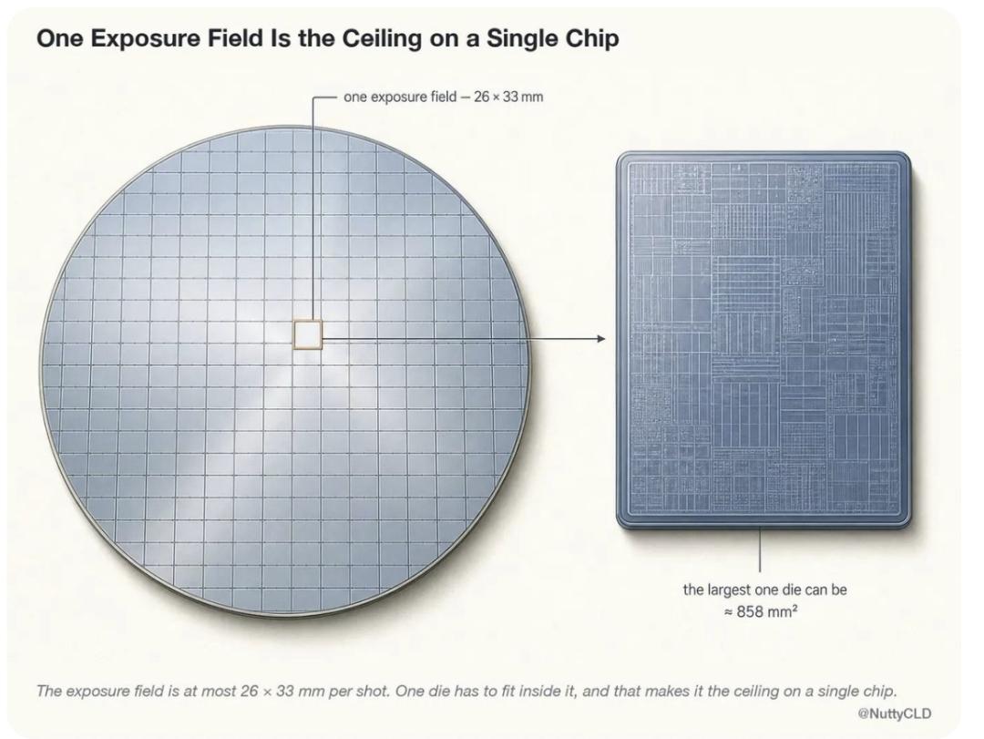
TSMC has achieved mass production of CoWoS packaging, with an exposure size 5.5 times that of ordinary packaging, capable of accommodating up to 12 HBM stacks, with a reported yield of over 98%. The roadmap released by TSMC at its North America Technology Symposium in April 2026 shows that its packaging size will reach 9.5 times in 2027 and 14-field in 2028. TSMC describes the 14x exposure field packaging as approximately 10 large computing chips plus 20 HBM stacks. Photoresist limits the size of individual chips, and the industry has broken through this limitation by packaging multiple chips in one package, which is exactly the development direction of packaging technology.
Profit Calculation:
Splitting Alone Only Reaches Break-Even Point
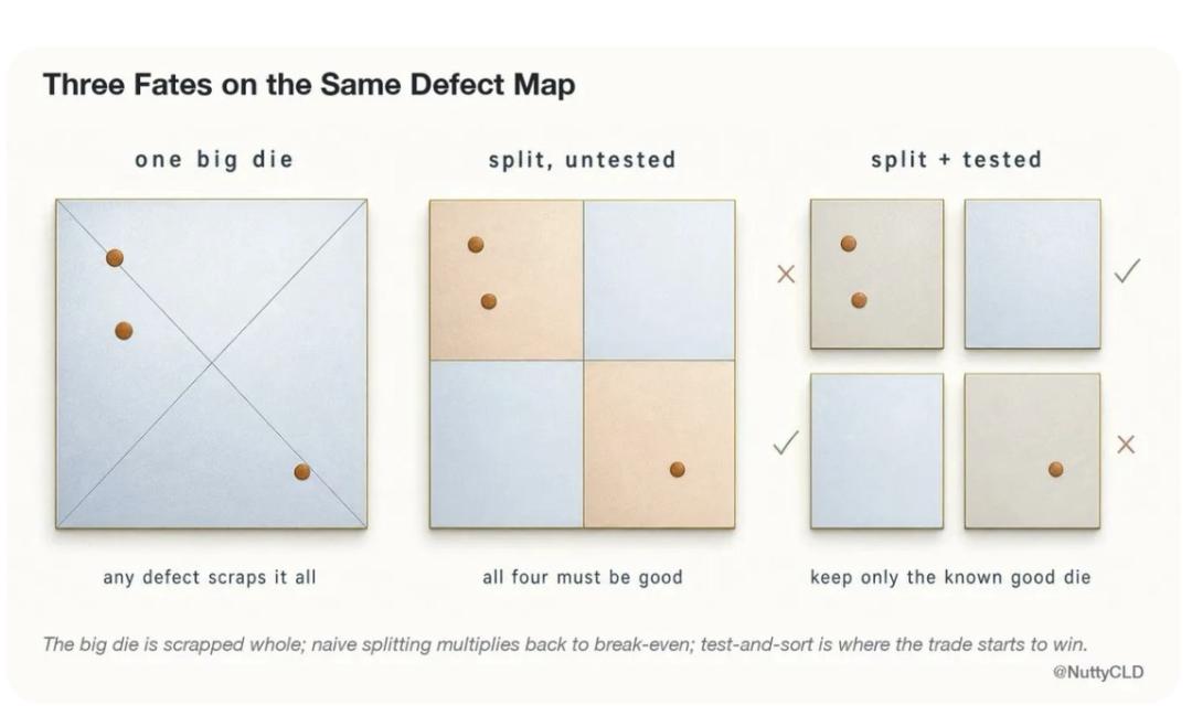
The second common reason for splitting chips is yield, but there is a widespread misunderstanding here. Manufacturing defects appear almost randomly on the wafer, so a larger chip means a higher probability of defects. Assuming the defect density is 0.1 per square centimeter, the calculation shows that the pass rate of a large 800-square-millimeter chip is about 45%, while the pass rate of a small 200-square-millimeter chip is about 82%. So is it really cost-effective to split a large chip into four pieces? All four chips must be qualified, which means multiplying 0.82 by itself four times, and the result is still 45%. As far as splitting chips alone is concerned, the gain is exactly at the break-even point.
The real advantage lies in the ability to test each component before assembly. The dies on the wafer can be probed one by one, and unqualified chips can be eliminated in advance. Qualified chips are called known good dies, or KGD for short. In the past, one defect would scrap the entire 800-square-millimeter processor, but now it only results in the loss of one 200-square-millimeter component. Reducing the loss unit from the entire product to a single component is the core of chip economics.
In fact, chip designers have been playing this game inside individual chips for a long time. The H100 physically contains 144 computing units, but NVIDIA only enables 132 of them: the reserved capacity ensures that no matter which unit has a defect, it will be shut down, and the rest of the units can still be delivered as a complete product. Cerebras uses the entire wafer as a single chip, taking this principle to the extreme, shrinking each core to 0.05 square millimeters, so that the impact of defects is limited to that exact scope. Chiplet extends the same principle beyond the chip boundary and brings two additional advantages. Components that do not require cutting-edge processes, such as I/O or cache, can be manufactured using cheaper mature nodes, and components verified once can be reused in other products. The mask size limit prompted the emergence of Chiplet; KGD sorting and node mixing made it profitable.
The Problem Has Not Disappeared,
But Has Shifted Into the Package
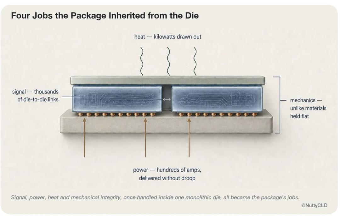
However, splitting chips does not make engineering design easier. The four tasks that were originally completed inside a monolithic chip now fall on the packaging layer. It must realize thousands of short and dense signal connections to ensure that all parts still work like a single chip; it must transmit hundreds of amperes of current without voltage drop; it must dissipate several kilowatts of heat; and it must firmly bond materials with mismatched thermal expansion coefficients (such as silicon, copper, organic substrates and packaging materials) under various temperature changes.
The more chips are stacked, the more severe the heat dissipation problem becomes. A simulation result released by the Belgian semiconductor research institute imec at the end of 2025 confirms this point: when HBM is directly stacked on the GPU (3D stacking) without any heat dissipation measures, the hot spot temperature reaches as high as 141.7°C; while the same silicon chips are placed side by side under the same heat dissipation conditions (2.5D stacking), the temperature remains at 69.1°C. The moment stacking is completed, the heat of the lower chip must be transferred to the upper chip. This is not just a simulation result.
The zHBM concept chip demonstrated by Samsung at the Hot Chips 2026 conference eliminates the interposer and stacks DRAM directly on the processor, which directly exposes it to heat dissipation problems. Samsung is trying to solve this problem by keeping the number of stacked layers at a low level (about four chips), mainly to reduce heat dissipation costs and avoid forming a single hot spot by dispersing I/O interfaces across the entire chip surface. At the same conference, Samsung's Heat Path Block technology and SK Hynix's iHBM technology also tried to solve the centralized heat dissipation problem from another perspective. Both technologies open up a dedicated heat dissipation channel in the interface area where heat accumulates. All of these are just attempts rather than finished products, and Samsung has not given a launch timetable for zHBM.
The bottleneck never disappears. It only shifts, and where it lands becomes the next equipment market.
The first step of the bottleneck stems from mask and yield calculation, that is, the wiring between chips. After that, the bottleneck continues to shift, and each step brings a question: from which vendors must the industry start purchasing equipment and materials?
Consequences Brought by This Transformation
For fifty years, packaging has been a low-margin and tedious part of the semiconductor value chain. A wafer worth tens of thousands of dollars comes out of the fab, undergoes probe testing, thinning, and dicing, then is sent to a packaging plant in Penang (Malaysia) or Kaohsiung (Taiwan). The packaging plant only needs to solder a few wires, encapsulate the chip in a plastic shell, perform testing, and then ship it, with negligible cost. The entire packaging equipment market is worth approximately... 5 billion U.S. dollars in 2025, within the current range guided by the wafer manufacturing equipment market of 150 billion to 160 billion U.S. dollars in 2026. No one studied it because there was nothing worth writing about.
The above physical principles put an end to this possibility. A single chip cannot economically break through the limit of one exposure field, and the closer it gets to this limit, the more waste it generates. The only solution is to print multiple smaller chips and stitch them together on the same substrate, a process called advanced packaging. Since the speed of this connection now determines the performance of the chip, packaging technology has evolved from a low-cost encapsulation process to one of the most critical technologies in the AI field. And since only one manufacturer (TSMC) can reliably assemble these chips on a large scale, this factory determines who can sell AI chips.
The backend has become the allocation mechanism for global AI computing.
CoWoS allocation is the way computing resources are rationed: it is estimated that NVIDIA will occupy more than half of TSMC's CoWoS quota, about 630,000 wafers in 2026, and will increase to about 1 million wafers in 2027 according to supply chain conditions; Broadcom ranks second, while MediaTek, AMD and hyperscale data center operators share the remaining quota. TSMC said they will not choose between customers and will not give up any business, adding that despite all their efforts, supply remains very tight. According to different definitions, the supply-demand gap in 2026 is expected to be between 10% and 20%. The data in June only includes accelerators, while the data in July incorporates the demand for server CPUs into the same queue. Without access to CoWoS quotas, AI chips cannot be delivered, and the increase in wafer capacity will not change this.
Today, the packaging business has become the top revenue source for one of the world's most important companies, TSMC: TSMC's backend revenue has risen from about 2.5 billion U.S. dollars in 2023 to 7.5 billion U.S. dollars in 2024, and is expected to reach around 12 billion U.S. dollars in 2025-2026. The proportion of advanced packaging products in TSMC's sales will grow from about 9% in 2026 to 16-18% in 2030. TSMC is already the world's largest packaging company, and is consolidating its position with a 50% growth rate.
The flow of funds has changed: ASE has raised its 2026 capital expenditure plan twice to 10.5 billion U.S. dollars, of which 70% of the equipment portion is used for cutting-edge packaging and testing. Amkor is investing heavily, putting 7 billion U.S. dollars into its Arizona plant. Intel requires customers to prepay for EMIB-T substrates, and in Intel's own words, customers responded enthusiastically with prepayments amounting to billions of dollars.
At the semiconductor conference in August, the clearest message from computing vendors was: supply, not demand, is the constraint; NVIDIA is actively locking in substrate and DRAM supply; AMD's growing server market share benefits both from the substrate capacity booked during the pandemic and its Venice architecture on the N2 platform. The supply chain determines revenue, and packaging is the supply chain.
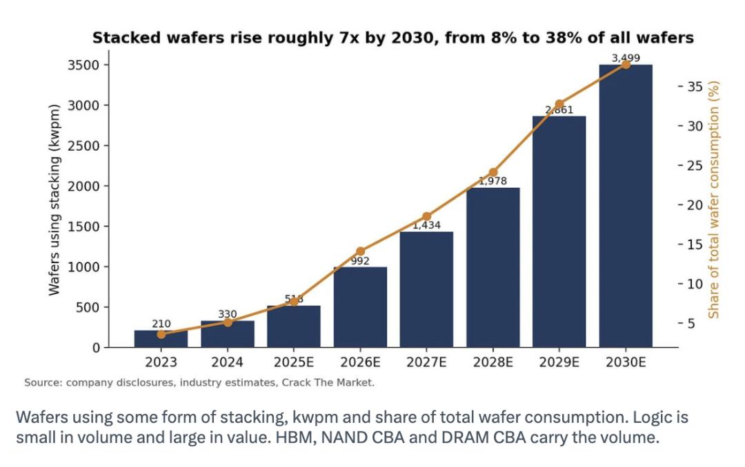
The scale behind this is not dominated by NVIDIA alone:
By 2025, about 518,000 wafers per month use some form of stacking technology, accounting for about 8% of all wafers.
By 2030, this figure is expected to reach about 3.5 million wafers per month, accounting for 38% of the total output of the entire industry, among which HBM, NAND CBA and DRAM CBA will dominate the output, while logic chips carry the value.
The tool and consumable companies serving this market are not in a cyclical fluctuation, but are experiencing a platform reshaping of the way the entire industry assembles products.
What Is Advanced Packaging?
Why There Are Several Times Differences in Published Data?
Published estimates for the same market range from less than 200 billion U.S. dollars to more than 500 billion U.S. dollars this year, with annual growth rates ranging from 11% to 59%. Why are the differences so large? Because they are counting different contents, so let's map out the value chain of advanced packaging.
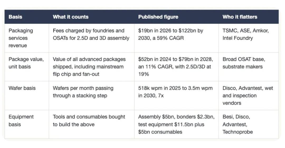
The level you focus on determines which companies look like winners:
Based on revenue, TSMC becomes the focus.
Based on production volume, the scale of OSAT (Outsourced Semiconductor Assembly and Test) looks larger than it actually is.
Based on wafer volume, the rise of Disco seems unstoppable.
Based on equipment, the entire industry looks very small, which is why ordinary investors ignore it.
Conclusion: The truly important number is capital expenditure, not revenue.
For investors at the equipment and materials level, the correct denominator should be the expenditure of packaging vendors, not their revenue, because payments to equipment suppliers come from expenditures, and expenditures come earlier and are stronger than revenue. Only two large OSATs have expenditures of about 13 billion U.S. dollars this year. TSMC allocates 10-20% of its mid-year raised capital expenditure budget to advanced packaging. Intel has allocated a large part of its increased capital expenditure to EMIB-T, and memory manufacturers are expanding HBM TSV capacity, targeting approximately 760kwpm by the end of 2027. Capital expenditure in the advanced packaging field easily exceeds 20 billion U.S. dollars every year, growing faster than wafer manufacturing equipment, and is concentrated in a small number of suppliers.
Disassemble the Advanced Packaging Supply Chain
It should be noted that due to the rapid development of the packaging industry, its market share data is usually only valid for about one year. To disassemble the advanced packaging supply chain, the easiest way to understand is to divide the process of chips from design to final system into five layers, plus a design layer that runs through all layers. Each layer has its own economic benefits, market share and certification cycle.
Materials: Ajinomoto's ABF thickening film is used in almost all high-performance packaging, with a market share of over 95%, and the company announced a 30% price increase in May. Nittobo's T-glass cloth is used to control the warpage of substrate core materials. ABF substrates themselves are manufactured by companies such as Ibiden (accounting for 70-80% of Blackwell substrates), Unimicron, Shinko, Nan Ya PCB, AT&S and Kinsus. Resonac provides die attach films for dicing, while Kao occupies about 60% of the substrate cleaning agent market share.
On the packaging vendor side: TSMC's 3DFabric platform (CoWoS, SoIC, InFO and WMCM) is the reference architecture and also the bottleneck. Intel Foundry provides EMIB, EMIB-T and Foveros packaging. Samsung provides turnkey HBM packaging services and has its own glass interposer product line.
On the OSAT vendor side: ASE (in partnership with SPIL) is the largest vendor and the only one with wafer-level advanced capital expenditure. Amkor is the local US alternative and Intel's first external EMIB assembler. JCET, TFME and Hua Tian Technology are Chinese vendors. KYEC, Sigurd and Ardentec are testing specialists.
Equipment: Bonders come from Besi, Hanmi, ASMPT, Kulicke & Soffa, SEMES, Hanwha, Shinkawa and Shibaura. Grinders and dicers come from Disco and Tokyo Seimitsu. Wafer bonders come from EV Group, Tokyo Electron and SUSS MicroTec. Packaging lithography equipment comes from Canon, Ushio and Nikon. Wet process equipment comes from GPTC and Scientech. Molding equipment comes from Towa, Yamaha Robotics and Besi. TSV etching and plating equipment comes from Lam Research and Applied Materials, CMP equipment comes from Applied and Ebara, temporary bonding and debonding equipment comes from SUSS, Tazmo and Tokyo Electron. Dispensing and thermal bonding equipment comes from All Ring, Nordson and Musashi.