TSMC bets on optical chips
TSMC's entry into the optical chip market is no secret.
Some analysts point out that TSMC's increasingly prominent position in the field of silicon photonics is expected to dominate the sector just as it does in the field of advanced artificial intelligence packaging. Leveraging its manufacturing platform COUPE (Compact Universal Photonics Engine), TSMC can combine cutting-edge electronic logic, mature photonics processes and advanced packaging integration, and its system-level integration capability is currently unmatched by competitors.
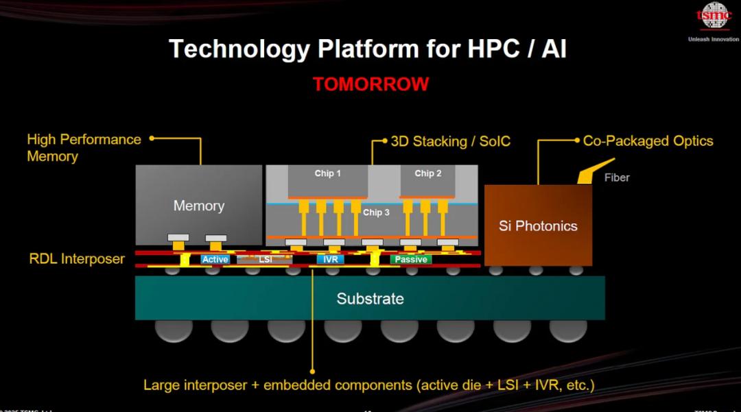
TSMC stated that compared with traditional microbump packaging solutions, COUPE technology can reduce power consumption by 40% at the same speed, or achieve a 170% speed increase at the same power consumption. More broadly, the optical device development roadmap shows that the energy consumption per bit will gradually decrease from more than 30 pJ/bit of traditional copper packaging to less than 5 pJ/bit for co-packaged optical devices on the substrate, and eventually drop to less than 2 pJ/bit as optical I/O moves to the interposer.
Recently, TSMC shared their latest insights into the optical platform.
Initial Optical Planning
Before introducing TSMC's latest progress, let's first review TSMC's planning for optical chips.
It can be seen from relevant introductions that TSMC's silicon photonics platform "COUPE" is based on SoIC technology. This system uses copper-to-copper bonding and hybrid bonding technology to directly connect electronic circuits (EIC) to photonic circuits (PIC) on the wafer. Allegedly, this photonic circuit contains all key components, including an advanced 200G microring modulator (MRM). Next, a layer of oxide is deposited on the wafer, which is then bonded to another silicon wafer. Finally, tiny holes called dielectric vias are created from the backside to establish electrical connections to the substrate.
Relevant reports point out that the modulator is another key component of PIC, which mainly includes microring modulator (MRM) and Mach-Zehnder modulator (MZM). Mach-Zehnder modulators (MZM) perform well in high-speed, high-power application scenarios, while microring modulators (MRM) have the advantages of compact structure and high density — making them the core component for efficient CPO transmission.
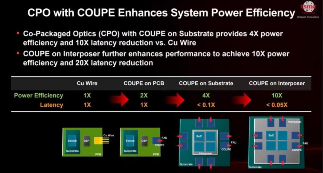
At the 2025 IEEE ECTC conference, TSMC's Silicon Photonics Division published a new paper that further reinforces the COUPE concept
TSMC stated that to meet the growing demand of bandwidth-intensive applications such as artificial intelligence and high-performance computing, a new broadband optical engine (BOE) architecture has emerged, which combines silicon photonics with advanced packaging technology. This optical engine integrates three key components at the system level — COUPE (Compact Universal Photonics Engine), COI (Complementary Optical Interconnect) and iFAU (Integrated Fiber Array Unit) — to implement co-packaged optics (CPO) in the 2.5D CoWoS environment.
The core of this architecture is COI, which is the key component to realize low-loss optical signal routing. COI consists of paired optical couplers and precisely designed structures, which can efficiently redirect the light from the iFAU fiber to the on-chip waveguide and guide the signal to the silicon photonic chip. This coupling path is critical for minimizing insertion loss and achieving high-performance optoelectronic co-integration.
A notable feature of the BOE system is its compatibility with wafer-level manufacturing. This process-oriented approach not only supports scalable bandwidth density (leveraging multi-wavelength operation and multi-row fiber arrays in iFAU), but also ensures high manufacturability through in-line process monitoring. By adopting a vertical optical coupling configuration, the system has higher fault tolerance for chip warpage — a major challenge in the field of advanced packaging. Unlike edge coupling (EC), which is highly sensitive to mechanical alignment, vertical coupling has higher robustness and stability under actual assembly conditions.
To verify the performance of the BOE platform, TSMC conducted a series of optical measurements on an entire 300mm wafer. Subsequently, the measurement results were compared with simulation and modeling data to evaluate performance consistency and identify process sensitivities. Studies have shown that the difference between the model-predicted optical performance and the measured optical performance is significantly affected by multiple critical dimension (CD) parameters, including waveguide width, etching depth, sidewall profile, surface smoothness and alignment accuracy.
These findings highlight the importance of strictly controlling the manufacturing process of optical devices. Even tiny deviations in structural dimensions or material properties will lead to measurable differences in optical loss and signal fidelity. As TSMC continues to expand its CPO capabilities through the CoWoS and SoIC platforms, integrating robust BOE technology is critical to achieving next-generation bandwidth density and system-level efficiency.
TSMC's Latest Updates
At the Optical Forum held in Chinese Taiwan yesterday, Hsu Kuo-chin, Vice President of Advanced Packaging Technology Development at TSMC, stated that the underlying architecture of optical transceivers is undergoing structural transformation, silicon photonics has become the mainstream form, and the market share is expected to exceed 50% in 2027. The ultimate embodiment of silicon photonics is co-packaged optics (CPO), and manufacturers will start mass production in the second half of this year.
He pointed out that with the exponential growth of artificial intelligence, networks are being pushed to their physical limits. Today's computing unit is no longer a single server, but the entire data center. And the nervous system of the data center is optics. Optical transceiver sales in 2025 increased by 25% compared with 2024, and it is expected to grow by another 50% in 2026. Among them, the high-end market with speed of 100G and above doubled in 2024, and will grow by another 60% in 2025.
Hsu Kuo-chin said that in 2028, the large-scale deployment of artificial intelligence will further trigger massive growth; in response to development trends, the underlying architecture of optical transceivers is undergoing permanent structural transformation. Silicon photonics has become the mainstream form, and its market share is expected to exceed 50% in 2027.
He pointed out that the semiconductor industry has fully invested in silicon photonics technology. Wafer foundry can scale up the production of optical engines.
Chen Ming-fa, TSMC's Deputy Project Director, also stated at the same forum that from the perspective of development trends, AI computing power grows about 3 times every two years, but I/O performance only grows about 1.4 times every two years. The gap between the two is gradually widening, and how to continuously improve I/O performance has become the key that must be solved for further expansion of AI systems.
To break through the I/O wall limitation, it is necessary to gradually shift from traditional copper transmission to optical transmission. Chen Ming-fa pointed out that traditional copper wires cannot support long-distance signal transmission in high-frequency environments, while optical transmission can effectively extend the signal transmission distance, further support AI data centers to realize Scale-up and Scale-out architectures, and meet the bandwidth and connectivity requirements of large-scale AI computing.
According to reports, there are currently two main architectures for integrating optical components into systems: one is CPO (CPO on Substrate), that is, the optical engine is integrated on the substrate; the other is OOI (Optical on Interposer), which integrates the optical engine onto the XPU. Compared with traditional copper wires, CPO and OOI technologies can bring about 4 to 10 times improvement in power efficiency and reduce latency by about 10 to 20 times.
TSMC is also actively developing optical platforms at present. As mentioned above, one of the representative technologies is COUPE, which adopts TSMC's SoIC-X bonding technology to integrate EIC and PIC through Bond-to-Bond method, and is equipped with TSMC's self-designed optical path structure.
COUPE supports two coupling methods: grating coupler (GC for short) and edge coupler (EC for short). Among them, in the key structure, silicon lens, metal reflector (MR for short), Si/SiN grating coupler can be seen from COUPE-GC; COUPE-EC has core structures such as EC facet and Sin Tip.
To support customers in designing photonic integrated circuits, TSMC also provides a complete component PDK, covering key components such as optical waveguides, bends, couplers, modulators and photodetectors, helping customers carry out silicon photonics design more efficiently, while shortening product development cycles and time to market.
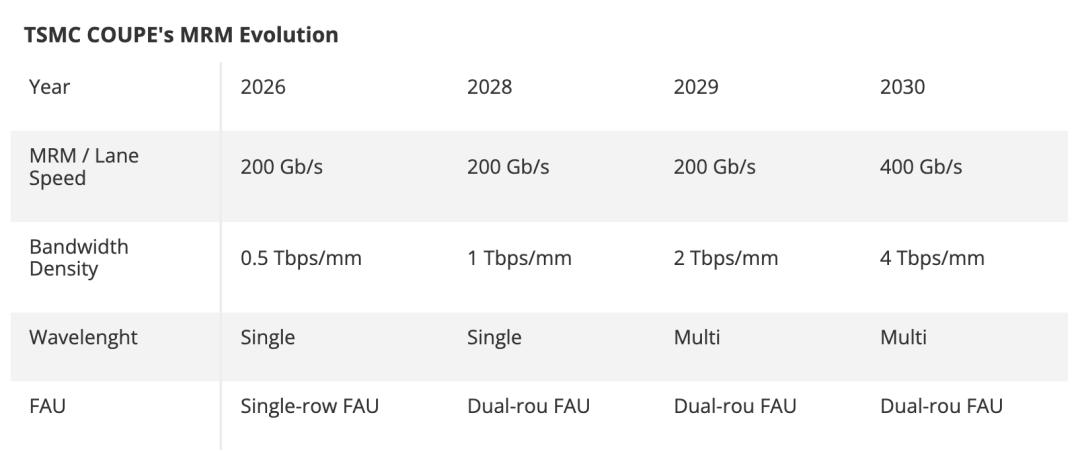
How can COUPE further expand the bandwidth? Chen Ming-fa said that there are currently two main bandwidth expansion strategies. The first is the "Fast and Narrow" strategy, whose core is to focus on increasing the transmission speed of a single Lane from 200 Gbps to 400 Gbps, and may even exceed 400G in the future. At the same time, TSMC will also expand the number of Lanes from 64 Lanes to 128 Lanes or even more, increasing the total bandwidth from 3.2 Tbps to 12.8 Tbps or even higher.
The second is the "Slow and Wide" strategy. The focus is not on extremely increasing the transmission speed of a single Lane, but on increasing the number of WDM wavelengths to expand the total bandwidth. WDM can be gradually increased from a single wavelength to 4, 8, 16 wavelengths or even more, to continuously expand the overall optical transmission capacity.
With these goals in mind, TSMC is continuously improving the performance of COUPE. In the next stage of development, the role of heterogeneous integration will become more important. Chen Ming-fa said that in the future, it is expected to directly integrate modulators, SOA (Semiconductor Optical Amplifier) and light sources onto the backside of the COUPE platform, further improve the integration degree of optoelectronic components, and provide more flexibility for subsequent system expansion.
Future Evolution Roadmap
According to Tomshardware reports, TSMC's silicon photonics technology roadmap is currently divided into three stages, from 1.6 Tbps optical engines using traditional pluggable optical devices to 12.8 Tbps optical engines integrated inside the processor package. The COUPE roadmap is closely related to TSMC's advanced packaging technology and the evolution of microring modulators (MRM), which are used to adjust light and directly affect performance. Therefore, several of TSMC's customers (such as NVIDIA) have formulated their silicon photonics strategies around the evolution of COUPE.
The first stage of the roadmap — named "COUPE on PCB" — adopts TSMC's SoIC-X bonding technology to bond 65nm electronic integrated circuits (EIC) with photonic integrated circuits (PIC). The initial target application of this solution is the OSFP (Octal Small Form-factor Pluggable) optical module, which can provide 1.6Tbps bandwidth (twice the throughput of copper Ethernet solutions and twice the energy efficiency). Therefore, the first-generation COUPE is not within the scope of this discussion. TSMC said that the SoIC-X interface has extremely low impedance, which can reduce power consumption while transmitting high-speed signals.
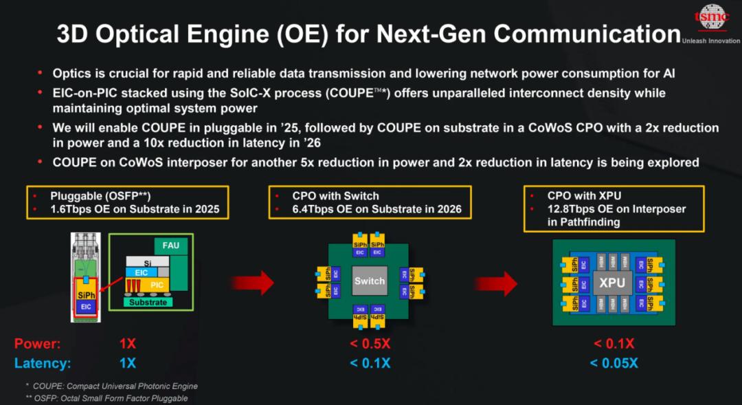
The second-generation product — named Substrate-based COUPE — marks TSMC's transition from traditional pluggable optics to co-packaged optics (CPO). At this stage, COUPE is integrated with TSMC's advanced chip packaging technology (CoWoS) and co-packaged with network switch ASICs. This architecture enables motherboard-level optical interconnection with a total bandwidth of up to 6.4 Tbps, 2 times higher energy efficiency, and 10 times lower latency than existing pluggable solutions, which is ideal for various applications such as NVLink, Ethernet and InfiniBand switches.
The third stage — named "COUPE on interposer" — pushes silicon photonics further into computing chips: a 12.8 Tbps optical engine is directly integrated into the processor package to achieve ultimate bandwidth and scalability. In addition to doubling the bandwidth again, the company expects the architecture to be 5 times more energy efficient and 20 times lower latency than current pluggable solutions. This will make it very attractive to hyperscale data center operators building clusters of thousands of accelerators.
In short, the main goal of COUPE is to connect the optical engine with the computing unit as closely as possible.
During the speech, Chen Ming-fa also emphasized that COUPE can also be used as an optical interposer. Chen Ming-fa explained that just like CoWoS-S, COUPE can support a maximum reticle size of 3.3 times, leaving a lot of room for imagination for various possible applications of COUPE in the future.
Chen Ming-fa further pointed out that as the demand for bandwidth, transmission distance and power efficiency of AI and HPC continues to increase, optical I/O will become a noteworthy technical solution; TSMC will also continue to optimize the COUPE platform to further support different optical transmission applications such as CWDM and DWDM; in the future, COUPE and CoWoS packaging will be further integrated, and may be applied in different fields. However, to realize a complete optoelectronic integration ecosystem, in addition to the technological development of the wafer foundry itself, close cooperation between all stakeholders in the industrial chain and OSAT players is also required.
But as Hsu Kuo-chin said, including lasers, optical fibers, fiber connectors and product testing, are becoming the real bottleneck for large-scale deployment.
This article is from the WeChat official account "Semiconductor Industry Observer" (ID: icbank), author: Editorial Department, 36Kr is authorized to republish it.