Chip giants are flocking to CPO
Recently, NVIDIA's Spectrum-X Ethernet Photonics CPO switching chip has been announced to be in full mass production, with the first batch of products delivered to CoreWeave, Lambda Labs and Oracle, making it the world's first 200G/lane CPO switch system to achieve large-scale commercial application.
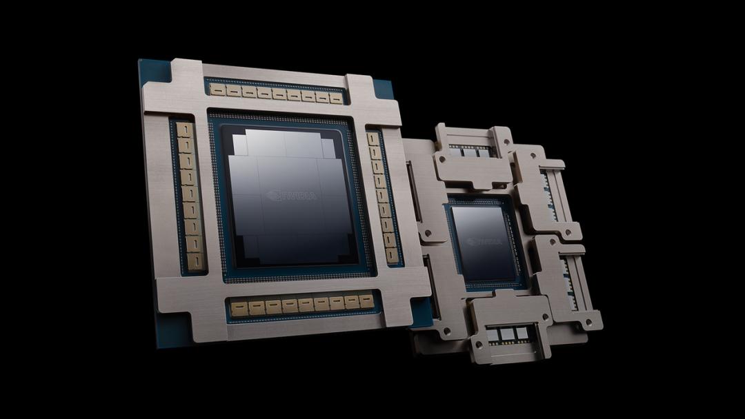
The significance of this milestone goes far beyond the launch of a single product. It marks that CPO (Co-Packaged Optics) has officially stepped out of the laboratory, evolving from a long-term industry roadmap to a practical option for AI data centers.
Almost at the same time, SK Hynix, in collaboration with top global academic institutions, published a CPO technology roadmap paper in *Nature Electronics*, pushing the battlefield of optical interconnection further from the network to the memory interface.
One focuses on computing power and the other on storage, both placing their bets on the same direction of CPO by coincidence — this is by no means a random occurrence.
Another noteworthy point is that there have been continuous dynamics in the CPO field recently: AMD disclosed the CPO roadmap for the MI500 accelerator, TSMC accelerated the ramp-up of PIC production capacity, Samsung released the complete plan for its 300mm silicon photonics foundry platform, GlobalFoundries entered the supply chain as a pure silicon photonics foundry, and Intel continued to promote the layout of compute-native optical I/O...
All the world's top chip and foundry enterprises have joined the competition, and a technical race around next-generation computing power interconnection has fully kicked off.
The Dilemma of Electrical Interconnection: Why We Must "Pursue Optics"
To understand why CPO has suddenly become a must-win battlefield for giants, we first need to see clearly the physical ceiling that traditional solutions are hitting.
As we all know, data transmission between traditional chips relies on copper wires to transmit electrical signals. Inside the data center, the electrical connection between the optical module and the switch chip already consumes more than 30% of the overall power consumption. When an electrical signal travels through a copper wire, the longer the distance and the higher the rate, the greater the energy consumption.
As data rates move toward 800G and 1.6T, the distance that copper wires can support is getting shorter and shorter. The data cited by SK Hynix is more intuitive: computing performance increases by about 3 times every two years, while interconnection bandwidth only increases by 1.4 times. This scissors gap, known as the "bandwidth wall", is tightening the ceiling of AI expansion.
The architecture logic of traditional pluggable optical modules is very simple: the switching ASIC chip outputs electrical signals, which travel through more than ten centimeters of PCB copper wires to the optical module on the front panel, and the electro-optical conversion is completed inside the module. The problem lies in this "long copper wire". The longer the electrical signal travels on the copper wire, the more serious the loss. In order to "recover" the signal, a DSP signal compensation chip is required, which has extremely high power consumption. When the cluster scales from ten thousand cards to one hundred thousand cards, the number of switch ports reaches tens of thousands. After a large number of ports are stacked, the extra power consumption and signal loss will become a heavy burden on the entire computing power cluster.
It is foreseeable that the traditional separated architecture of "switching chip + pluggable optical module" is approaching the physical limit of copper-based electrical interconnection.
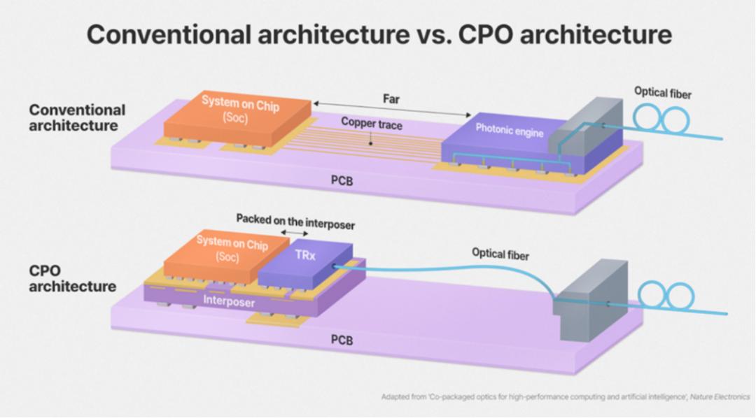
CPO moves the optical engine closer to the processor, increasing bandwidth and energy efficiency by shortening the transmission distance of electrical signals (Source: SK Hynix)
The essence of CPO is architectural reconstruction: the silicon photonic engine (PIC), switching chip, and computing chip are packaged on the same substrate, so that the optical interface is closer to the chip, or even directly adjacent to the chip. The transmission distance of electrical signals is compressed from more than ten centimeters of PCB traces to the level of several millimeters. As soon as the electrical signal comes out of the computing chip, it is immediately sent to the optical engine to complete electro-optical conversion.
This change brings a systematic performance leap:
Greatly improved energy efficiency: Official data from NVIDIA shows that compared with traditional pluggable solutions, the overall power consumption of Spectrum-X is reduced by about 80%, the link loss is reduced from 22dB to 4dB, and signal integrity is improved by 64 times.
Centralized light source: Adopting the ELS external centralized light supply architecture, the number of lasers is reduced by 75%, which not only reduces the cost, but also reduces the number of failure points synchronously, and the mean time between failures of the equipment is increased by about 10 times.
Leap in bandwidth density: After getting rid of the limitation of panel physical space, more optical channels can be integrated in a single package, supporting a switching capacity of 102.4Tb/s per chip and even 409.6Tb/s for the whole system.
The deeper significance is that CPO allows optical interconnection to truly enter the interior of the package for the first time, becoming an advanced system integration technology alongside 2.5D/3D packaging and HBM stacking, rather than just a board-level peripheral.
Chip Giants Compete for CPO
CPO is not a single technical standard, but a route competition around "how to co-package optics and electronics". Global leading chip and foundry enterprises have taken different strategic paths based on their own endowments.
NVIDIA: First to Pull the Trigger on Mass Production
NVIDIA is one of the most aggressive promoters of CPO commercialization at present, and also the only system vendor that has achieved large-scale shipments.
It was first released at the GTC conference in March 2025, included in the Vera Rubin platform in January 2026, put into production at the end of May, and announced full mass production on August 14 — from concept to mass production, it took NVIDIA only one and a half years for CPO.
It is reported that the first batch of customers include heavy players in AI computing infrastructure such as CoreWeave, Lambda Labs and Oracle, and cloud service providers such as Microsoft Azure, Meta and Nebius have also confirmed adoption.
Spectrum-X Ethernet Photonics is built based on the new generation Spectrum-6 switching chip, with a single chip switching capacity of 102.4Tb/s, twice that of the previous generation Spectrum-4. The flagship model SN6800 stacks 4 ASICs in a 5U chassis, with a total bandwidth of 409.6Tb/s, supporting 512 800Gb/s ports.
What is more noteworthy is the reasons behind the performance data. Compared with traditional pluggable solutions, NVIDIA's CPO solution reduces the number of lasers by about 75%, reduces the overall system power consumption by about 80%, increases the mean time between failures by 10 times, reduces the maximum link loss from about 22dB to about 4dB, and improves signal integrity by about 64 times.
NVIDIA's determination is not only reflected in products. In July 2026 alone, NVIDIA invested a total of 2 billion US dollars in two optical companies, Coherent and Lumentum. Together with other layouts, it has built an optical strategy of about 4 billion US dollars.
On the whole, CPO is not just an upgrade of network equipment, but an extension of NVIDIA's GPU ecosystem. By deeply binding switches with GPUs and network software, NVIDIA is pushing the AI cluster from the hybrid mode of "GPU + white-box switch" to a full-stack integrated closed ecosystem, further raising customer migration costs.
SK Hynix: From HBM to "Optics-Centric"
Recently, SK Hynix, a giant famous for memory chips, published an optical interconnection paper in *Nature Electronics* — this move is a signal of the escalating competition in the AI computing power industry chain.

SK Hynix is a core supplier of HBM, which solves the memory wall at the chip level — no matter how strong the GPU computing power is, it will not work if data cannot be fed in. But when the cluster scale expands to the cabinet level and data center level, optical interconnection becomes the next bottleneck.
SK Hynix's layout of CPO is essentially an extension from "on-chip bandwidth" to "inter-cluster bandwidth".
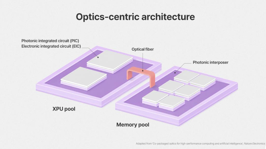
Schematic diagram of the "optics-centric" architecture proposed by SK Hynix. Computing resources and memory resources form XPU pools and memory pools respectively, connected by optical fibers and photonic interposers. (Source: SK Hynix)
It is understood that the most forward-looking part of the paper is the proposal of an "optics-centric" architecture. In the current architecture, electrical signals are still used for connection between HBM and GPU, and physical space constraints limit the number of HBM stacks that can be integrated in the package. The optics-centric architecture directly connects the computing resource pool and the memory resource pool with optical signals through a photonic interposer, bypassing physical space constraints. Its core value lies in "memory pooling" — multiple accelerators can share a memory pool that is much larger than what a single package can accommodate.
SK Hynix's research team has set clear technical goals for next-generation AI infrastructure: single-node bandwidth exceeding 100Tb/s, energy consumption lower than 1pJ/bit, and inter-chip latency lower than 10 nanoseconds. The roadmap clearly outlines the evolution path from 2D and 2.5D interposers to 3D heterogeneous stacking.
More notably, SK Hynix revealed that the next phase will explore ultra-large-scale parallel optical interconnection based on Micro LEDs. Although this is still in the technology R&D stage, it shows that the memory giant's layout of optical interconnection is far more far-reaching than the outside world imagines.
TSMC: Core Backend Production Capacity, COUPE Defines Mass Production Standards
If NVIDIA and SK Hynix are the chargers on the CPO track, TSMC is the "chief engineer" who builds the infrastructure behind the scenes. As the process base for the vast majority of CPO solutions, TSMC is the absolute dominant player in current silicon photonics production capacity, and its COUPE platform has become the industry's mass production benchmark.
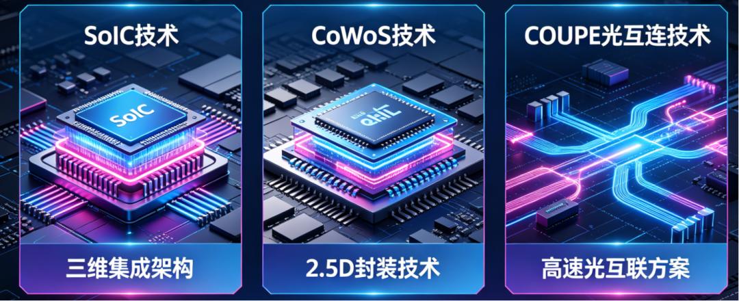
TSMC launched the compact universal photonic engine COUPE technology in 2021. COUPE adopts SoIC-X bump-less copper-copper hybrid bonding technology, placing the electronic chip directly on top of the photonic chip, which can achieve ultra-low impedance at the inter-chip interface and higher energy efficiency. Performance verification shows that compared with lead-bonded 3D microbump interconnection, its signal rate is increased by 70% and power consumption is reduced by 40%.
TSMC claims that COUPE achieves a 5-10x improvement in power efficiency and a 10-20x reduction in latency through its interposer integration architecture.
TSMC's ambition goes far beyond technology. According to reports, TSMC is negotiating to acquire two LCD panel factories owned by AUO in the Central Science Park, with the transaction amount expected to exceed NT$30 billion. What TSMC really values is not the LCD production capacity, but the large-size manufacturing capability behind these plants — directly renovating existing panel factories can shorten the construction cycle by several years, and quickly build large-size packaging production capacity at the 510×510mm level.
The pace of TSMC's capacity expansion is also amazing.
According to estimates from legal persons, TSMC's PIC production capacity will rapidly increase from about 500 wafers per month in early 2026 to 10,000 wafers per month in the second quarter of 2026, then increase to 15,000 wafers per month in the fourth quarter, and increase to at least 25,000 wafers per month in 2028. If calculated at 648 dies per wafer, the monthly production capacity of 25,000 wafers corresponds to an annual PIC output of about 194 million units.
TSMC's approach essentially regards optical I/O as another Tile of 3DFabric: SoIC handles vertical stacking, CoWoS handles 2.5D wiring and coexists with HBM, and COUPE is responsible for the chiplet on the optical port side.
From 2026 to 2027, the main mass production customers of the COUPE platform may be leading enterprises such as NVIDIA, Broadcom and AMD. After the capacity expansion in 2028, CPO projects of MediaTek, Marvell, Ayar Labs and other manufacturers may be introduced one after another.
Samsung: HBM + Silicon Photonics Combined Play, Launching Storage-Aware CPO
Samsung entered the CPO race a little later and is a "chaser" in this competition, but its strategy is the most systematic, trying to play a set of combination punches — a differentiated "vertical integration card", relying on the full-chain capabilities of storage, wafer foundry and advanced packaging to take the route of integrating storage and optical interconnection.
In March 2026, Samsung officially released its 300mm silicon photonics foundry platform at the OFC conference, announcing its entry into the optical communication market, and released a complete roadmap for the optical communication foundry platform. The roadmap is divided into four steps: complete CPO mass production preparation in 2026; realize mass production of optical engines based on thermal compression bonding technology in 2027; transition to EIC-PIC vertical stacking with hybrid copper bonding in 2028; and officially provide "turnkey" CPO full-process foundry services in 2029.
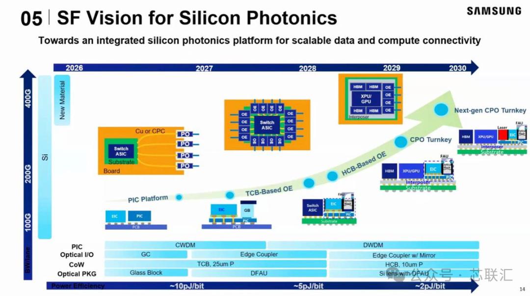
Source: Corelink
This means that by 2029, Samsung