Hot Chips is on a rampage, with HBM, CPUs and GPUs all pulling off incredible feats that rewrite their destinies against all odds.
At this year's Hot Chips, the competition remains extremely fierce.
If there is one most intuitive feeling, it is that in previous Hot Chips events, participants preferred to talk about technology trends and paint grand visions, but this year the sense of rivalry is far more obvious: various manufacturers have started to preview next-generation products, release roadmaps, and demonstrate architectural details. It is clear that the competition in the Agentic AI track is so intense that all parties are racing against time, and no one wants to fall behind.
However, manufacturers have presented a huge amount of content, covering CPUs, GPUs, HBM, interconnection, packaging, networking... the entire event is packed with technical details that are not easy to digest. Today, EEWorld will use the most concise and summarized language to clearly explain what the chip giants announced at Hot Chips and what they plan to do.
How HBM is Scaled Up to 16 Layers and 20 Layers
Most people are well aware of how drastically memory prices have risen, and the root of this price surge comes from HBM. At Hot Chips 2026, the focus of the first day is also HBM.
Micron has put forward a judgment: computing power increases by approximately 3 times every two years, while the growth rate of memory bandwidth is less than 2 times. What is the solution? Simply stack HBM to higher layers. But the problem is that the higher you stack, the more difficult it gets. Therefore, Micron, Samsung Electronics, and SK Hynix discussed two issues from engineering and academic perspectives this time: how high can HBM actually be pushed? Should HBM continue to be "stacked higher" unilaterally?
Currently, mainstream HBM mainly adopts 8-layer or 12-layer DRAM stacking. Samsung and SK Hynix have set their sights on 16 layers, 20 layers, or even higher. Micron believes that a relatively clear technical path for 16-layer HBM already exists, and 20-layer or higher stacking is not impossible, but challenges will rise rapidly once the layer count exceeds 16.
The core challenge lies in finding a new balance between higher capacity, higher bandwidth, and cost, power consumption, and heat dissipation. The next breakthrough for HBM may no longer be just the bandwidth bottleneck, but the physical limit of the entire system. 3D stacking and Hybrid Bonding have become unavoidable key terms, and at the same time, advanced packaging and heat dissipation technologies will also play a critical role.
Samsung: Proposes Truly 3D-Architected zHBM
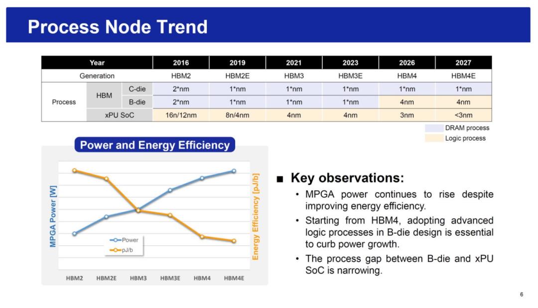
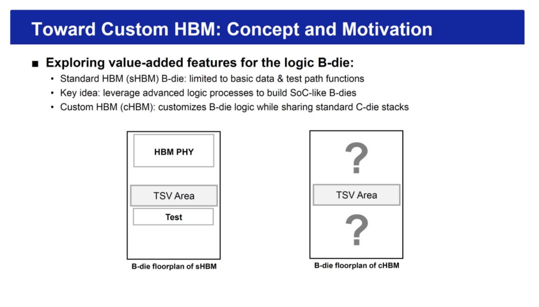
Samsung is the most aggressive manufacturer this year, drawing a very ambitious "vision" for HBM. The core change lies in the B-die (Base die), which is the base substrate at the bottom of HBM. In the past, B-die was mainly responsible for PHY, data paths, and testing. As AI computing power continues to improve, the continuous doubling of HBM bandwidth has begun to be restricted by the number and pitch of TSVs, as well as the quantity and rate of PHY I/Os. Therefore, Samsung has started to use advanced logic processes to revamp B-die: HBM4 has adopted D1c and 4nm processes to reduce power consumption and shrink the die area.
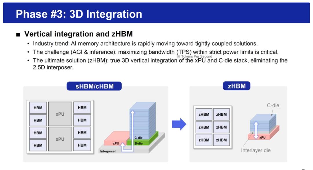
Samsung divides this roadmap into three steps: Custom HBM (CHBM) → Advanced HBM (aHBM) → zHBM (truly 3D integration).
cHBM is the current stage. By using advanced logic processes to replace the traditional HBM PHY with a more compact D2D interface, shortening the signal path, and moving part of the memory controller and other functions from the XPU to the B-die, freeing up area for the GPU. Samsung has also introduced HPB thermal path blocks, which can reduce the peak temperature by more than 35%. The goal of this stage is to reclaim 5% to 10% of the XPU area, bringing a 10% to 20% performance improvement;
aHBM is the transition stage. It will continue to use the unused area of B-die to add memory expansion controllers, RAS, testing functions, and even part of the Processing Elements. Especially as the context window of AI models continues to lengthen and KV Cache keeps expanding, B-die can connect to external memory for further capacity expansion; at the same time, moving part of the computation closer to the storage side can also reduce data movement, lowering power consumption and bandwidth pressure;
zHBM is the final goal Samsung is pursuing. It eliminates the traditional 2.5D interposer, directly stacks HBM vertically on XPUs such as GPUs, shortens the signal path through distributed I/O, and removes SerDes to further reduce power consumption. Samsung's targets are very aggressive: compared with HBM4E, zHBM delivers approximately 230% higher bandwidth, 70% better power efficiency, saves up to about 100W per single DRAM module, and targets an I/O power consumption of about 0.5pJ/bit. To achieve zHBM, Samsung is advancing advanced packaging technologies such as WoW (Wafer-on-Wafer) and HCB (Hybrid Cubic Bonding).
SK Hynix: Integrates Intel EMIB into its Roadmap
SK Hynix has also announced the packaging roadmap for next-generation HBM. Similar to Samsung, its focus is not only on "stacking HBM higher", but also solving bandwidth, power consumption, and heat dissipation issues through advanced packaging, and eventually moving towards 3D integration.
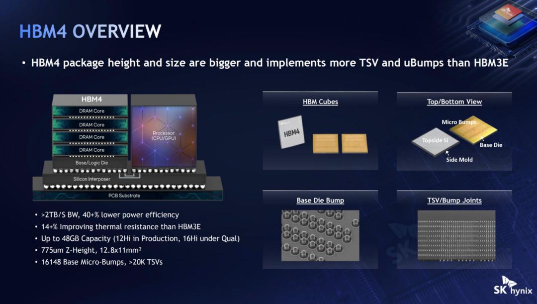
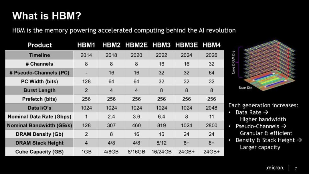
Currently, SK Hynix's HBM adopts 2.5D packaging: multiple layers of DRAM are stacked on B-die through TSVs, and then connected to XPUs such as GPUs through a silicon interposer. HBM4 has already achieved a bandwidth of over 2TB/s, a maximum capacity of 48GB, and integrates more than 20,000 TSVs. As bandwidth continues to increase, problems become more and more prominent: rising power consumption, increasing TSV count, worse heat dissipation, and expanding packaging area.
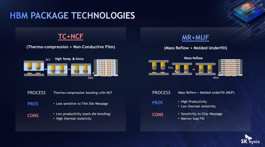
SK Hynix mainly uses two packaging solutions: TC+NCF and MR+MUF. On 16-Hi HBM3E, SK Hynix has adopted the upgraded MR-MUF technology, which raises the packaging height to 775μm through warpage control, finer-pitch interconnection, and narrow-gap filling, while further reducing die thickness, gaps, and bump pitch.
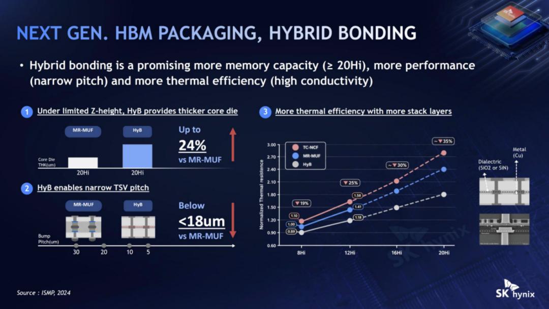
However, when moving towards higher stacking, traditional packaging alone is increasingly unable to meet requirements. Therefore, SK Hynix has started researching Hybrid Bonding. Compared with MR-MUF, hybrid bonding can support finer TSV pitch, with a target of less than 18μm. Even if the number of stacking layers continues to increase, the thermal resistance can still be reduced by about 35%. This means that future HBM is expected to break through the 16-Hi limit and continue to develop towards higher stacking.
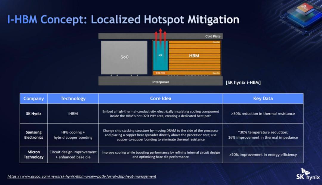
Heat dissipation is also a key priority. SK Hynix is developing its own hotspot solution I-HBM, adding high-thermal-conductivity, insulating heat dissipation materials to the D2D PHY hotspot area of HBM to build dedicated thermal paths, further reducing thermal resistance by more than 30%.
In terms of bandwidth, SK Hynix plans to continue increasing the number of TSVs, raise I/O rates, and introduce advanced logic processes. On the power supply side, it will improve PDN through advanced logic processes and more Power TSVs to reduce the power supply pressure brought by high-bandwidth HBM.
In addition to the packaging technology of HBM itself, SK Hynix has also demonstrated multiple 2.5D packaging solutions, including Intel EMIB, which is on par with CoWoS-S, CoWoS-L, and CoWoS-R. At the same time, SK Hynix has already set its sights on 3D integration.
As for whether HBM must be stacked higher, SK Hynix believes that the answer ultimately depends on the specific needs of AI training and inference. Especially in inference scenarios, data such as KV Cache needs to be accessed frequently, which has high requirements for both bandwidth and capacity, so customers hope to obtain HBM with high density and high bandwidth. But this does not mean that all data must be placed in HBM. The more likely direction in the future is to let HBM handle the most critical workloads with the highest bandwidth requirements, while other tasks are assigned to memory with larger capacity and lower cost such as LPDDR.
Micron: HBM Needs to Solve Heat Dissipation Problems
Micron stated at Hot Chips that once the layer count exceeds 16, there are two major challenges:
The first is cost. To achieve extremely high bandwidth, HBM requires a large number of parallel data paths, TSVs, and power supply structures. For the same capacity, HBM consumes far more silicon wafer area than DDR. For example, the wafer resource consumed per GB of HBM3E capacity is about three times that of DDR5. As bandwidth continues to rise, die size expands, and the number of stacking layers increases, this ratio does not show a clear trend of improvement in the short term.
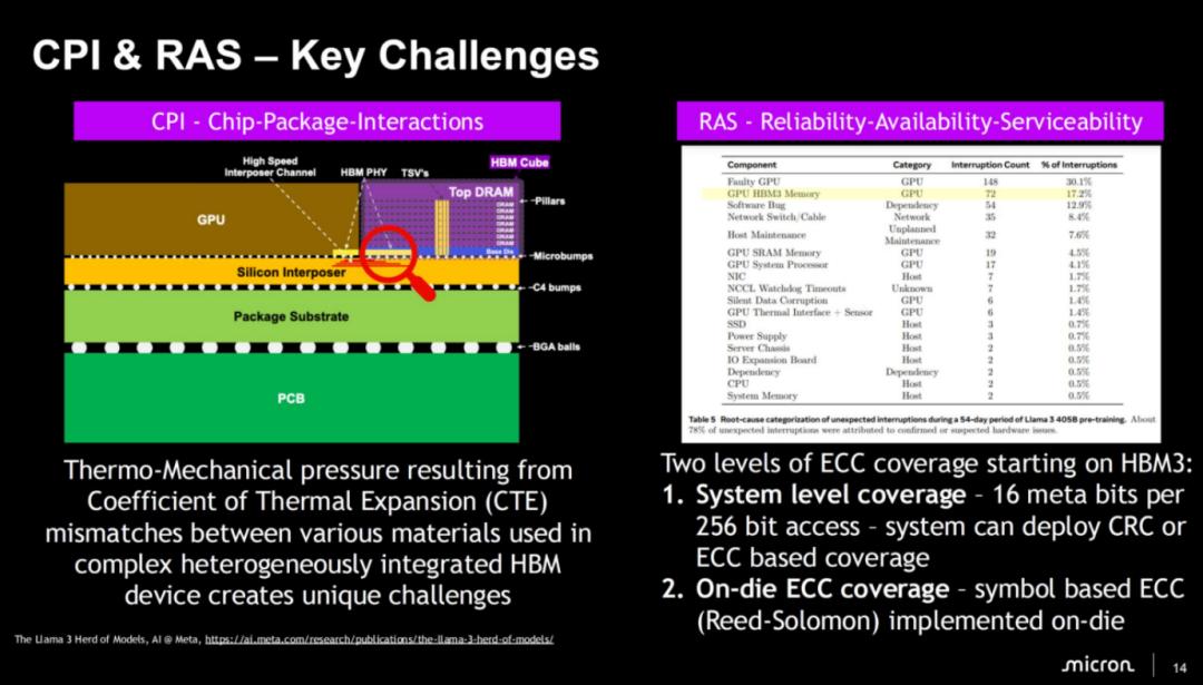
The second is heat dissipation. The Base Die of HBM integrates high-speed D2D interfaces and more and more logic functions, which is often the area with the highest power density in the entire HBM, and has become one of the regions most prone to hotspots in HBM. The increase in stacking height not only means higher thermal resistance, but also brings more mechanical reliability and manufacturing issues.
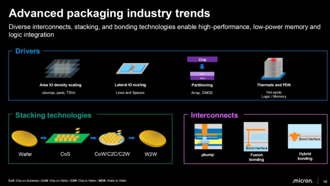
Therefore, for HBM to continue to develop towards 20 layers or even higher in the future, the key is no longer just making DRAM thinner, but how to solve a series of problems such as thermal management, packaging reliability, and manufacturing yield. This is why hybrid bonding is gaining more and more attention. Compared with traditional connection methods, more advanced interconnection technology is expected to reduce structural restrictions and improve inter-die connection and thermal conduction.
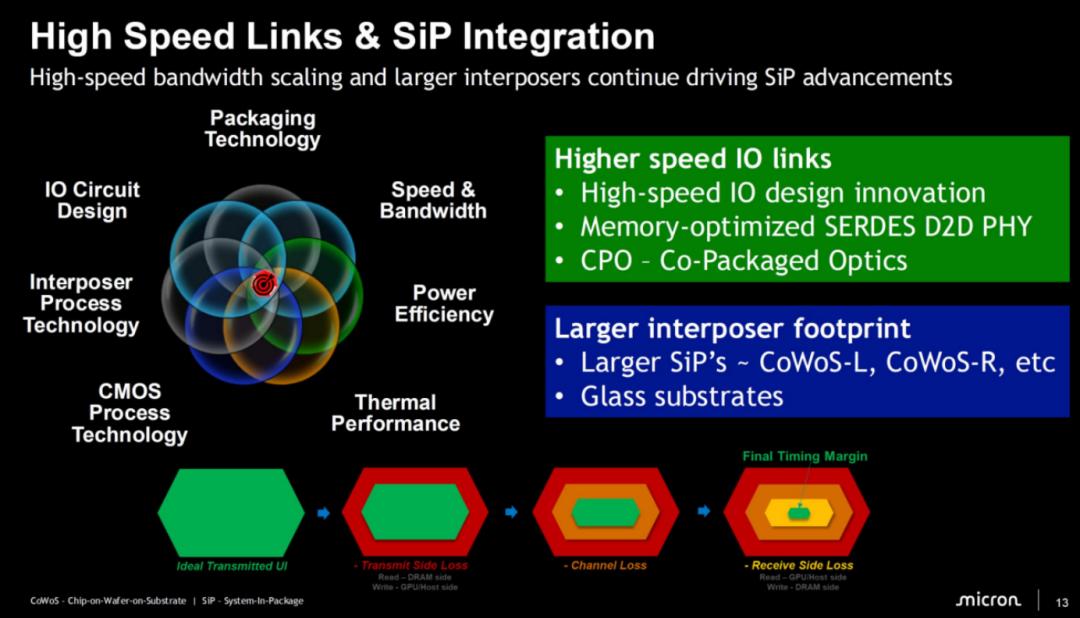
Micron believes that future HBM upgrades must advance three paths simultaneously: first, continue to increase bandwidth and capacity; second, redesign high-speed I/O; third, solve heat dissipation problems through advanced packaging.
Micron is advancing higher-density Fusion Bonding. Compared with traditional Microbump, Hybrid/Fusion Bonding can achieve smaller connection pitch, allowing more data to be transmitted inside the package, while reducing the thickness of the dielectric layer between DRAM layers and lowering thermal resistance.
Micron also proposed that in the future, it is necessary to redesign high-speed SerDes optimized for memory, and continue to explore HBM stacking with more than 16 layers. However, Micron's judgment is also very cautious. 20-layer or higher HBM cannot be achieved by simply stacking a few more layers of DRAM. Mechanical stress, die warpage, heat dissipation, testing, and reliability will all become new challenges. Therefore, Micron believes that the competition for HBM in the future will essentially become more and more like a comprehensive engineering of "chips + packaging + materials".
HBF is Also Entering the Arena
There are no official HBM products on the market yet, but at Hot Chips 2026, many experts are conducting simulations and predictions around HBF (High Bandwidth Flash), focusing on discussing how it can be used for AI workloads. Currently, SanDisk and SK hynix are promoting this technology.
AI models are getting larger and larger, and the demand for DRAM capacity is also increasing. HBM is becoming more and more expensive, and the AI industry needs an alternative path. The cost per GB of DRAM is much higher than that of NAND Flash, so the concept of High Bandwidth Flash (HBF) has become popular. In the future, NAND may no longer only be the "storage medium" in SSDs, but officially become