HBM reaches a crossroads
At the Hot Chips conference, both Samsung and SK Hynix agreed that GPUs, memory, wafer manufacturing, and packaging must be designed as a unified system. Since then, their solutions have gone separate ways.
Samsung is transforming the base die into an active part of the system. It plans to move the memory controller off the GPU and onto the logical base die, freeing up 5–10% of the GPU area for more computing and potentially boosting performance by 10–20%. Selective AI operations can also run on the base die to reduce data movement. In the long run, it is pushing zHBM technology, which directly stacks the GPU and DRAM, expected to cut DRAM power consumption by about 70% while more than doubling bandwidth.
SK Hynix, on the other hand, focuses on higher stacking and managing the resulting heat and warpage issues. It confirmed that 12-layer stacked HBM4 has entered mass production, while the 16-layer version has reached the customer verification stage. Hybrid bonding is the path to 20-layer and higher stacking, allowing for thicker dies and tighter pitches. Its iHBM approach adds a dedicated thermal conduction path inside the hottest area of the stack. This competition is no longer just about bandwidth and capacity. Base die architecture and advanced packaging have become the decisive battlefields.
Samsung's Custom Base Die Built on Logic Nodes
During its 2026 Hot Chips presentation, Samsung Electronics unveiled zHBM, the ultimate evolution of high-bandwidth memory. This concept abandons the 2.5D interposer, vertically stacking DRAM directly on top of computing chips such as GPUs to form a true 3D integrated architecture, with the goal of reducing DRAM power consumption by 70% and boosting bandwidth 2.3 times compared to HBM4E.
Samsung has laid out a three-phase roadmap to transform the base die from a passive data transmission channel into an active computing partner. The first phase moves the memory controller from the xPU to the base die to reclaim silicon area; the second phase adds memory expansion and attention computing capabilities to the base die; the third phase ultimately delivers zHBM.
Next, let's take a look at Samsung's solution.
At the beginning of the presentation, they provided several charts showing the development trend of HBM5 in terms of specifications. While nothing is set in stone, the chart in the upper right corner is quite interesting to examine.
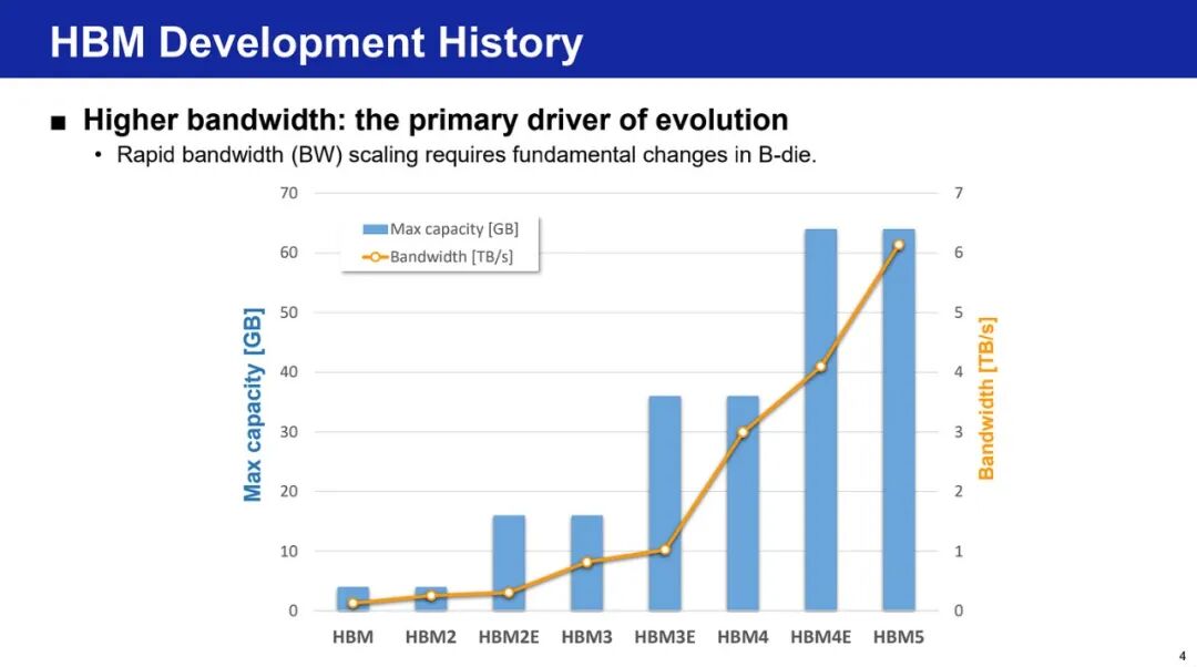
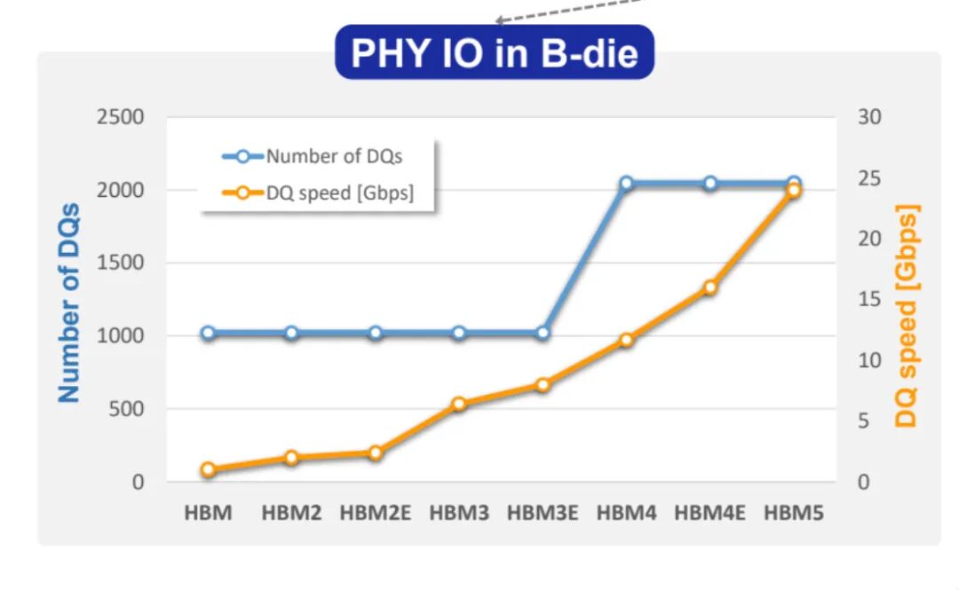
An HBM5 SSD with 60GB capacity and 6TB/s bandwidth is quite impressive. Let's work out the specific figures. 6 TB/s of bandwidth with 2048 channels means a transfer rate of 23.5 Gbps per pin. Our current state-of-the-art speed is 16 Gbps, which is a huge leap, and this is very likely to be achieved with advanced logic nodes. If each die has a capacity of 3 GB and the total capacity is 60 GB, the stack height will be 20 layers.
On another slide, Samsung confirmed that the per-pin transfer rate of HBM4E is 16 Gbps. Our earlier calculations for HBM5 are also verified in the figure below.
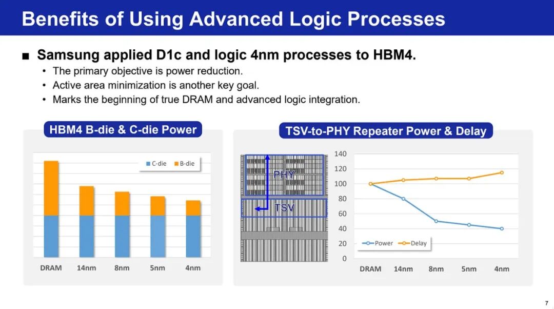
Samsung's obvious advantage is that it develops its own logic chips, while Micron and SK Hynix need to cooperate with others to obtain such chips. Samsung emphasized its own advantages here and explained the importance of custom chips. Samsung uses its 1C process to manufacture memory and 4nm process to manufacture logic chips, which significantly reduces chip power consumption. The figure below takes a subtle dig at Micron, which uses DRAM processes to manufacture logic chips in its HBM4 memory dies.
Even better, as mentioned earlier, Samsung clearly divides its product roadmap into three phases, which we will introduce one by one.
Phase 1: Low-Hanging Fruit
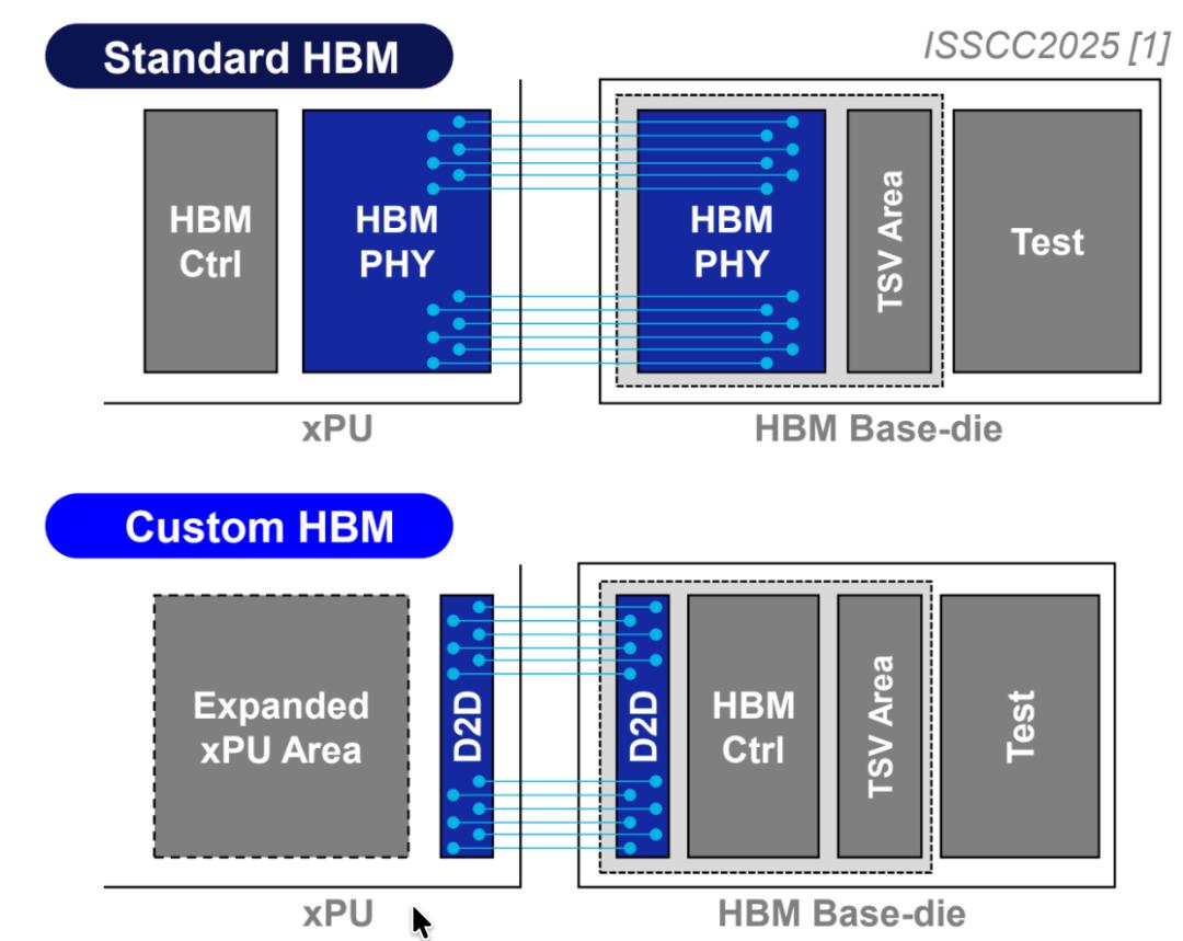
When the base die memory is built on a logic node, the physical area of the HBM PHY module shrinks, and energy efficiency also improves. This means the size of the inter-chip module connecting the HBM and XPU will be smaller. This brings two advantages:
Increase the area in the XPU for more computing;
Increase the available area of the HBM base die to enable more advanced functions.
The downside of the size reduction is higher thermal density in these areas. Interestingly, they provided the actual dimensions of the PHY modules in different generations of HBM.
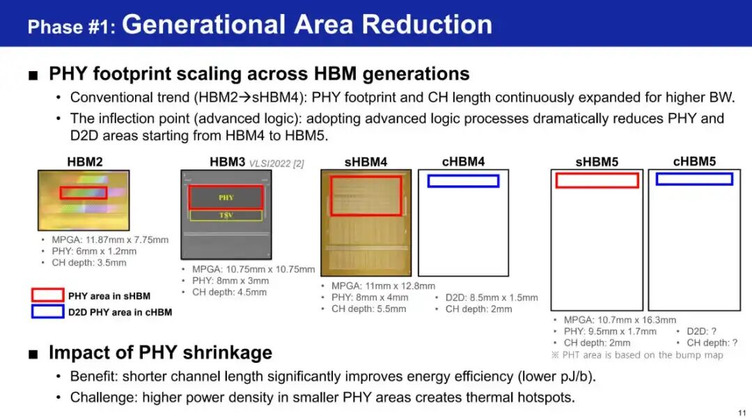
Samsung also mentioned that they do not tend to use UCIe in D2D links, as UCIe has a larger size and higher energy consumption per bit. They stated that their custom PHY implementation delivers better performance. When transitioning to HBM5, they presented the concept of an integrated Heat Path Block (HPB) for cooling the D2D PHY area.
Another major advantage is memory controller offloading, which can be moved from the XPU to a custom base die. This frees up space on the XPU die that can be used to deploy more floating-point operation processors.
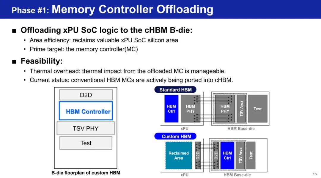
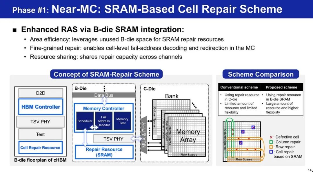
The new advantage of integrating logic nodes on the base die is the ability to implement SRAM. If a cell in the DRAM stack is damaged, the information in that cell can be temporarily stored in the SRAM, and the memory controller will retrieve the information from the SRAM instead of the damaged DRAM cell. You can think of the SRAM as a spare notebook, a temporary notepad for holding data that cannot be stored in the faulty DRAM cell.
Phase 2: RAS, Testing, Expansion, Processing
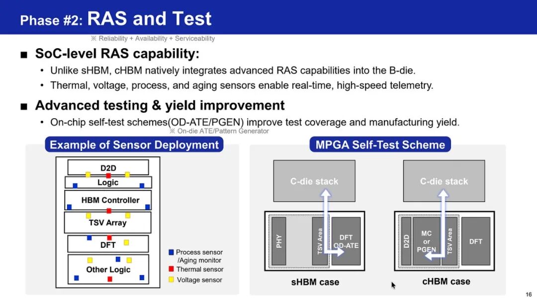
Using a logic node as the base die means that with smaller transistor sizes, the silicon area used for many of these functions will also be smaller. The saved space can be used for multiple purposes, such as improving the reparability, availability, and serviceability (RAS), running tests, and collecting telemetry data on the health/status of the HBM memory stack. Given that HBM telemetry issues are the second largest cause of training failures, HBM telemetry data will be extremely useful.
If there is still remaining silicon area, an additional memory expansion controller can be built to connect another HBM stack behind the first HBM stack, or insert DRAM dies to expand memory capacity.
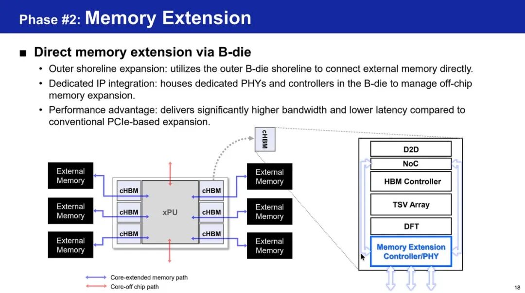
Finally, since logic transistors are available, why not integrate some computing functions on the base die as well? The benefit of this is that computations such as matrix compression or encoding can be completed on the logic die without leaving the base die, which brings advantages in both latency and efficiency.
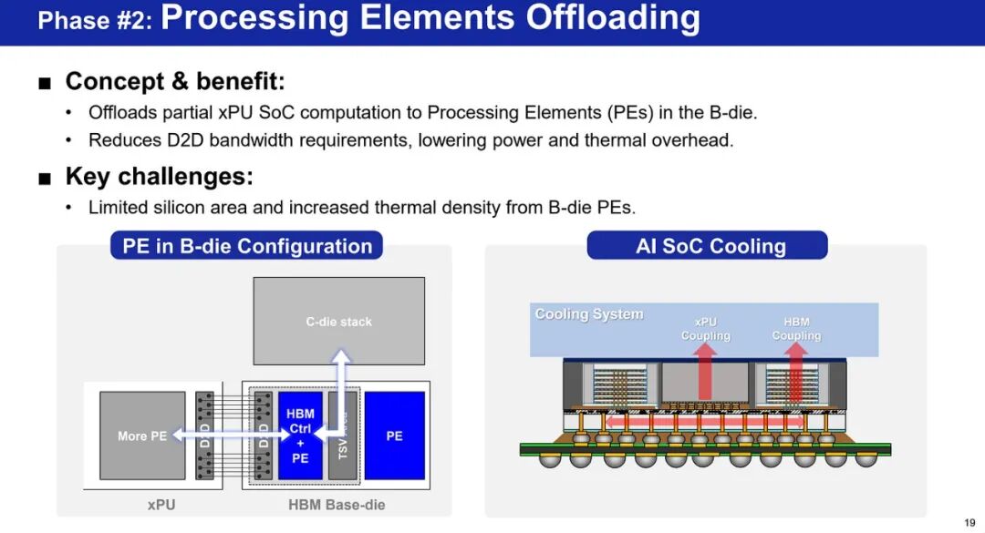
If everything goes well, the compact accelerator in the lower right corner can theoretically be constructed. Drawing such a block diagram is easy and conceptually interesting, but it remains doubtful whether its actual performance improvement will be significant.
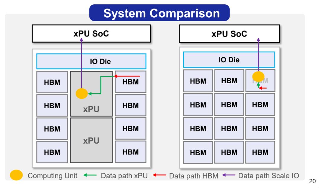
Phase 3: Vertical Integration
The final phase is to use custom base dies and HBM, and stack them on top of the logic dies. The distance between the computing die and the memory die is very short, so data bits only need to travel a much shorter distance, which improves energy efficiency and increases memory bandwidth by enabling more parallel data paths within the die area (not just at the die edge).
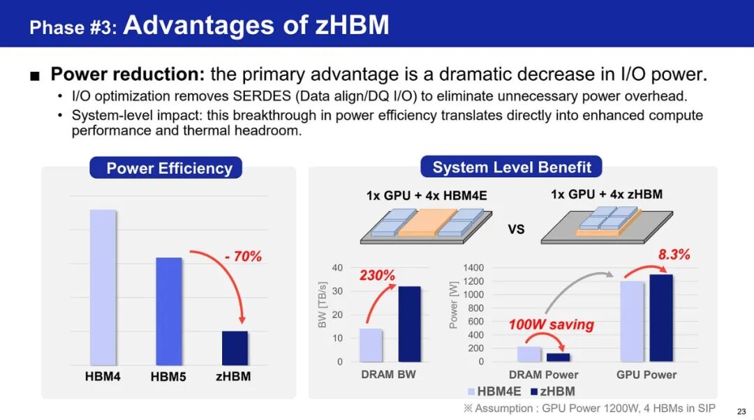
None of this is easy, but it is critical for companies to lay out a roadmap for technological improvement. This shows their confidence in launching better products in the future, which is a good thing for the company. As for whether the market is ready to adopt this product, that is another question.
SK Hynix Advances HBM5 Hybrid Bonding Technology
Jaesik Lee, Vice President of Packaging Engineering at SK Hynix America, said in his speech at Hot Chips 2026 on August 23 that SK Hynix expects hybrid bonding technology will not meet the requirements of HBM4E, which means the industry's most anticipated memory packaging transition will not happen until HBM5 at the earliest.
As he described, the problem is that the total thickness of the HBM cube is limited to 775 microns — the standard thickness of 300mm logic wafers — so each additional DRAM layer must use thinner dies and narrower gaps. The 16-layer high-density HBM4 currently undergoing customer certification (with a 48GB per-cube capacity, while the 12-layer high-density HBM4 is already in mass production) thins its core die to about 50 microns and halves the gap between dies. Lee's presentation also detailed the company's iHBM cooling architecture, launched three months earlier in May. Lee explained that the architecture has a limitation that the thermal modules cannot be applied to any HBM products that are already in the design phase.
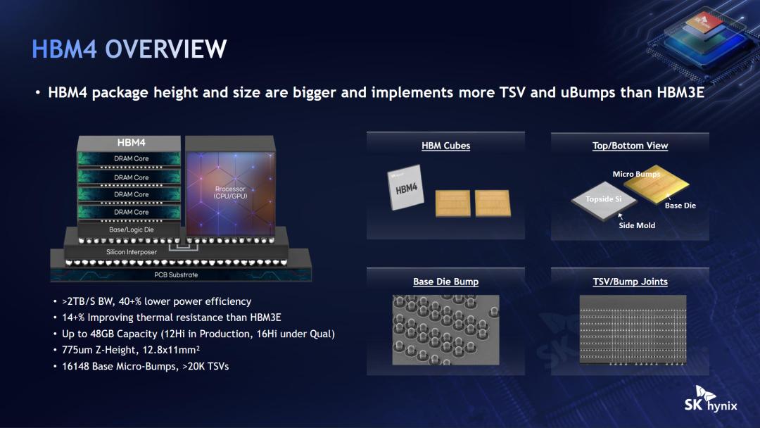
The JEDEC HBM4 standard raised the upper packaging thickness limit from 720 microns (inherited from HBM3E) to 775 microns, which eases the pressure of adopting hybrid bonding technology. Lee said that when the GPU package is fitted with a cold plate, both the logic die and the memory stack will be partially ground down to expose bare silicon. Since the logic wafer is 775 microns thick, if the height of the memory die increases further, it will exceed the height of the adjacent processor. "That's the limit we can currently reach, because the logic wafer is also 775 microns thick," Lee said.
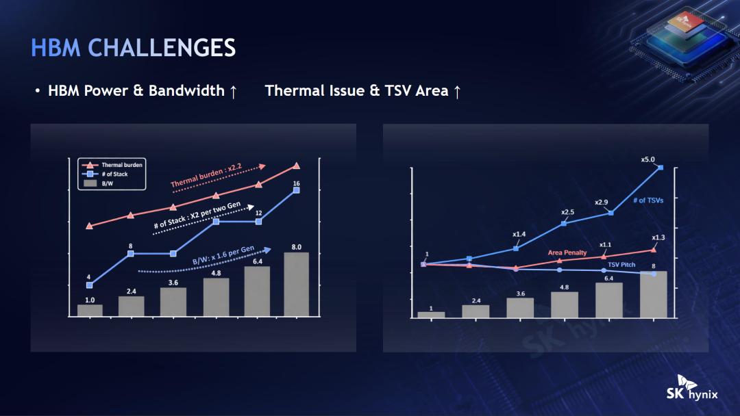
Thinner dies mean a higher proportion of oxide layers in the stack, and oxide layers have far lower thermal conductivity than silicon. In addition, the pin speed has increased from 1 Gbps in early HBM to 8 Gbps in HBM4, resulting in more power consumption in the same area. SK Hynix's own data shows that the thermal load across all shown HBM generations is 2.2 times higher on average, and the number of stack layers doubles every two generations.
The company's Mass Reflow Molded Underfill (MR-MUF) process, which stacks all dies via pick-and-place and connects them in a single reflow step, has already squeezed margins: according to Lee, filling the gap reduced by half while controlling the warpage of dies thinner than 50 microns is the major manufacturing challenge for 16-Hi stacks.
Last May, Samsung publicly committed to using hybrid bonding to produce HBM4, while SK Hynix positioned copper-copper bonding as an alternative to its advanced MR-MUF technology. Subsequently, JEDEC relaxed the thickness limit, making hybrid bonding