Storage chips, a new battlefield
Storage chips are evolving from standardized commodities to strategically customized components for AI infrastructure. This transformation is profound and irreversible.
Recently, the article titled "Intel Storage, Making a Comeback? It May Be Different From What You Think!" pointed out: A recent statement by Intel CEO Lip-Bu Tan on a podcast has caused quite a stir in the storage industry: "In the past, I always believed that storage was a low-margin commodity business that I would never touch; but the AI era is completely different, and we are developing a brand-new memory architecture."
A person who once voluntarily withdrew from the storage battlefield now announces his return in a high-profile manner — and the way of return does not seem to be resuming the old DRAM business, but betting on a brand-new customized memory architecture.
This signal is worth in-depth exploration.
Intel is not an isolated case. Samsung uses zHBM to reconstruct 3D memory; SK Group Chairman Chey Tae-won also said bluntly: Memory is no longer just a commodity that cannot be replaced by any other product, and put forward the slogan of "Creator of Full-Stack AI Storage"; Micron executives simply declared that memory is no longer an ordinary commodity in the bill of materials, and they cut off consumer brands to fully bet on the AI customization market.
The moves of leading manufacturers point to the same direction: The storage industry is shifting in an all-round way from standardized competition focused on production capacity and price to differentiated competition focused on architecture and customization, undergoing a paradigm shift from "general purpose" to "customization".
The Plight of General-Purpose Storage in the AI Era
To understand the current changes, we need to review the once-established rules of the game in the storage industry.
For decades, DRAM and NAND flash memory are the most typical "commodities" in the semiconductor industry. Samsung, SK Hynix, and Micron produce chips with unified specifications, and customers purchase on demand based on spot market prices or short-term contract prices. The products of different manufacturers are highly homogeneous and mutually substitutable. Once there is a slight imbalance between market supply and demand, prices will fluctuate drastically.
At the product level, storage chips have unified industry standards. JEDEC defines all specifications from interfaces, packaging to performance parameters. The product parameters, performance and specifications of various manufacturers are highly unified, with extremely strong versatility. From PCs, mobile phones to servers, a standard DDR memory stick and a general NAND particle can adapt to most scenarios, with differences only in capacity, speed and brand. Large-scale mass production and homogeneous competition are the mainstream of the industry.
At the technical level, the iteration paths are highly homogeneous — DRAM pursues more advanced processes to increase density and reduce power consumption; NAND competes for stacking layers to expand capacity and reduce costs. There is almost no disruptive change at the architecture level, and all optimizations focus on capacity expansion, slight speed improvement and cost reduction.
Corresponding to the business model, the industry follows a typical commodity cycle: focusing on selling standardized products in large volumes, price competition and large-scale supply chains. The core competitiveness of manufacturers is concentrated on yield, production capacity and cost control. The transaction logic of storage chips is very simple — the products of different manufacturers are highly substitutable. For purchasers, memory is only a general component in the cost structure; for original storage manufacturers, the only profit moat is to reduce the production cost per chip through economies of scale, and whoever can push the cost per bit to the lowest can survive at the bottom of the cycle.
The most typical manifestation of this generalized model is that storage chips have long been regarded as cycle products by the industry — when demand rises, the whole industry expands production, and when supply exceeds demand, prices plummet, and manufacturers then go through the cold winter together.
For decades, the storage industry has always followed the cycle of "price rise — production expansion — oversupply — price collapse". But the arrival of AI has completely broken this logic.
The first is the "memory wall" dilemma. Over the past two decades, processor performance has increased at a rate of about 60% per year, while the improvement rate of memory performance is only about 9%. The long-term unbalanced development speed has resulted in the storage speed seriously lagging behind the computing speed of processors. The number of parameters of Transformer models increases 410 times every two years, but the growth rate of GPU memory bandwidth is far behind. From NVIDIA H100 to B200, AI computing power has jumped from 4000 TFLOPS to 20000 TFLOPS, an increase of 5 times, but in the same period, HBM bandwidth only increased from 6.4GT/s to 9.6GT/s, an increase of only 50% — the gap between computing speed and data transmission speed is expanding rapidly.
The CEO of SK Hynix pointed out that the accelerated application of AI has led to an explosive growth in information flow, but storage performance has failed to keep pace with the progress of processors, forming the so-called "storage wall" obstacle. It is like a genius who has amazing thinking speed, but cannot record all ideas in time because he writes too slowly, and the final output efficiency is seriously dragged down.
In addition to the bandwidth bottleneck, the fragmentation of scenario adaptation also makes general-purpose storage stretched thin. The AI industry has long been divided into completely different demand scenarios: cloud large model training pursues extreme bandwidth and capacity, cloud inference values energy efficiency and latency stability, AI PC needs to balance performance and power consumption, and in-vehicle and edge AI have strict requirements for volume and temperature tolerance.
The sub-scenarios of the AI industry vary greatly, and the demand is naturally fragmented, so a set of standardized products cannot meet all of them at the same time.
Furthermore, there is the generational gap in architecture. Traditional storage architectures are designed for general-purpose computing, which cannot match the collaborative logic of AI computing chips, resulting in high data movement costs and extremely low system energy efficiency ratio. As industry experts said, the memory bandwidth that industry standards can provide has been basically clear in the next ten years, but the infinite demand for performance of modern AI systems is multi-dimensional, and its demand far exceeds the level that industry standards can meet.
The deeper risk lies in the business model. The production logic of traditional general-purpose storage is "mass production first, then sales". Manufacturers expand production based on cycle predictions and then supply the whole industry. But in the era of customization, storage manufacturers must intervene in customers' chip design processes in advance, and jointly define specifications with AI chip manufacturers.
Former Intel CEO Pat Gelsinger said bluntly that storage manufacturers may no longer simply mass produce standardized products in the future, but must turn to customized chips, and even start betting on which processor companies will become the winners in the future. A correct bet may bring stable customers for several years; a wrong bet may leave piles of high-cost, unsold chip inventories that no one is interested in.
It is against this background that the storage industry has begun a profound transformation from standardization to customization.
From Standardization to Customization,
Become the New Main Line of the Storage Industry
It can be seen that AI computing power demand forces the underlying innovation of storage and the transformation to the customization trend.
For a long time, the transaction logic of standard DRAM is very simple, and the products of different manufacturers are highly substitutable. But the emergence of HBM has broken this supply-demand paradigm. In order to meet the strict requirements of large models for data throughput rate, HBM needs to stack multiple layers of DRAM chips vertically and connect them to the underlying logic chips through thousands of through-silicon vias (TSVs). This physical structure determines that it is no longer a standardized part assembled independently, but must be highly bound to the packaging system of computing chips at the manufacturing stage.
An HBM chip goes through thousands of processes from wafer manufacturing, TSV drilling, micro-bump welding to advanced packaging, and the production cycle lasts for several months. The extremely complex manufacturing process not only raises the technical entry threshold, but also makes the product lose the general interchangeability of traditional memory.
This makes the value attribute of storage products being redefined.
In the past, storage chips were "commodities"; today, they are becoming core assets with strategic value in the AI industrial chain, and memory chips will become more customized products to better meet the needs of chip design companies.
Specifically, the transformation of customized storage is advancing along several directions:
From "general adaptation to all scenarios" to "exclusive optimization for a single scenario": The demand difference of different sub-scenarios of AI is much greater than the difference between consumer electronics and servers in the past. Training clusters require TB-level bandwidth and hundreds of GB-level capacity, inference nodes pay more attention to performance per watt and random read-write latency, and end-side devices strictly limit power consumption and volume. Standardized products cannot meet the extreme needs of any scenario, and only in-depth customization for a single scenario can break through the performance ceiling of the general architecture.
The explosion of ASIC demand pointed out in the Goldman Sachs research report is the best confirmation of this logic. Cloud vendors such as Amazon, Google, and Meta are accelerating the self-development of AI chips, and their memory solutions are fully shifting from general LPDDR and GDDR to customized HBM. The growth rate of ASIC-driven HBM demand will reach 82% in 2026, far exceeding the 23% driven by GPUs. The demand for storage customization of such self-developed chips is much higher than that of standardized GPUs.
From capacity priority to "bandwidth, energy efficiency, and architecture collaboration priority": In the era of general-purpose storage, larger capacity and lower price are the core selling points. But in AI scenarios, capacity is only a basic indicator. Bandwidth determines whether the computing power can run at full speed, energy efficiency determines the operating cost of the data center, and architecture collaboration determines the final system-level performance. The competitive focus of storage manufacturers has shifted from the cost per bit to the cost per unit bandwidth and system-level energy efficiency ratio.
From passive supplier to co-architect: In the past, storage manufacturers only needed to deliver products according to the specifications given by customers. Now, they need to deeply participate from the AI chip design stage, and jointly define the full-link specifications such as interface, packaging, power consumption and heat dissipation. SK Hynix clearly stated that the simple role of supplier is no longer sufficient to meet market demand, and storage manufacturers need to act as co-architects to exceed customer expectations in the field of AI computing.
The cyclical nature of the industry is greatly weakened: The traditional storage cycle is driven by consumer electronics demand, with a cycle of rise and fall every 3-4 years. But AI brings long-term, structural incremental demand, and customized products generally lock in orders through 3-5 year long-term agreements, which greatly smooths the cyclical fluctuations.
Gu Nozheng even directly put forward the assertion that "the storage cycle is dead": The storage cycle dominated by mobile phones and PCs, with rise and fall every few years, has completely ended. The permanent incremental demand brought by AI has completely rewritten the underlying logic of the industry cycle. Even after 2030, the overall global storage demand will still exceed the total production capacity.
When products move from standardization to customization, and when sales move from spot goods to long-term agreements, the "commodity" attribute of the storage industry is fading rapidly, replaced by a new positioning as a strategic AI infrastructure.
Storage Giants Are Competing Fully on the Customization Track
Under the wave of storage customization, the four giants of Intel, Samsung, SK Hynix and Micron have chosen different entry paths, and built differentiated competitive barriers respectively.
Intel: Return to the Track with Architecture Innovation
Intel's return to the storage market does not compete head-on with Korean and American giants in the mature HBM market, but directly lays out the next-generation new storage architecture, trying to reconstruct the technical route of high-bandwidth memory from the bottom.
Lip-Bu Tan has publicly stated on many occasions that he is focusing on promoting a new storage architecture project, whose core goal is to solve the storage wall problem faced by AI systems. Intel's layout is mainly carried out around two technical routes.
The first is ZAM (Z-Angle Memory). In February 2026, Intel reached a cooperation with SAIMEMORY, a subsidiary of SoftBank, to jointly develop this new architecture of high-bandwidth memory. The project was officially launched in Q1 2026, and it is expected to launch prototype products in 2027 and achieve commercial mass production in 2030.
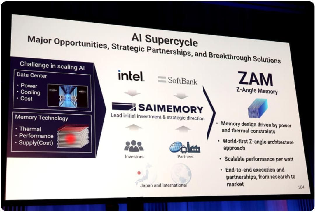
Source: PCWatch
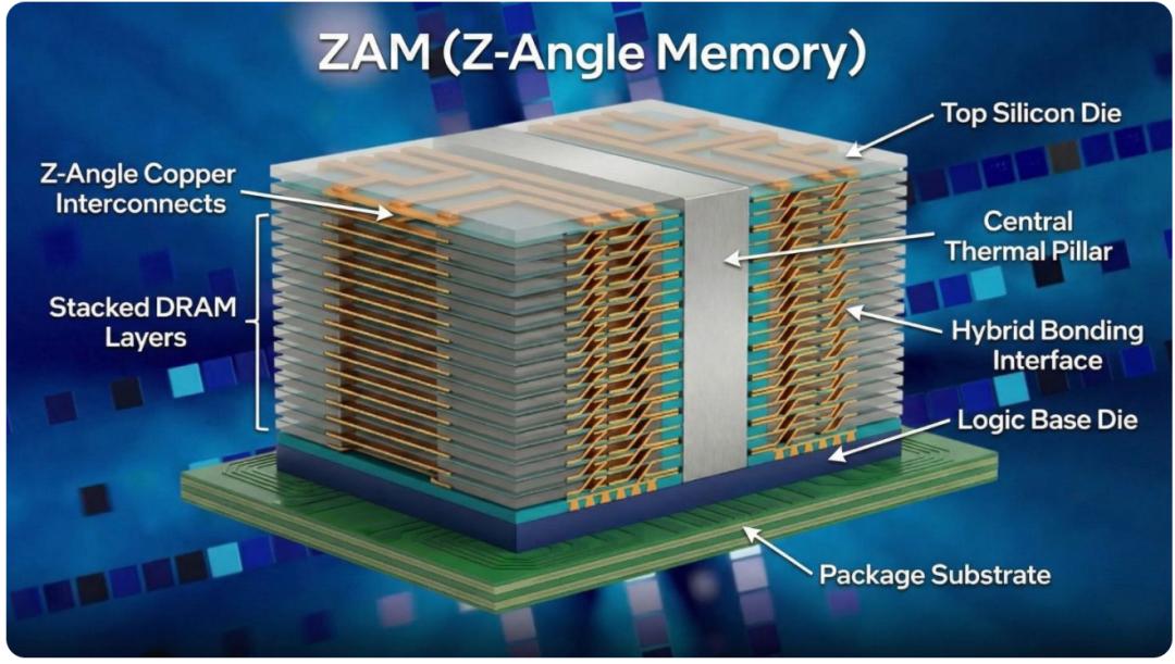
The core innovation of ZAM is that it abandons the traditional through-silicon via (TSV) design of HBM and adopts an oblique interconnection topology. This design can significantly improve heat dissipation performance and reduce interconnection power consumption. The official claims that the power consumption is 40%-50% lower than that of traditional HBM; the maximum capacity of a single chip can reach 512GB, which is 2-3 times that of the current mainstream HBM; and the mass production cost is only 60% of HBM.
Source: Xinjijia
In terms of structure, ZAM adopts a 9-layer stacking design, including 8 layers of DRAM chips and a 3μm thick silicon substrate spacer layer, which achieves a balance between density and heat dissipation.
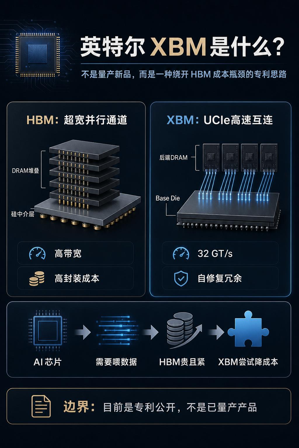
The second is XBM (Cross-Batch Memory). In July 2026, Intel published the relevant patent. This solution adopts back-end transistor DRAM stacking design, outputs data through UCIe interconnection, and the maximum rate can reach 32GT/s. The core goal of XBM is to eliminate the expensive silicon interposer necessary for HBM, greatly reduce advanced packaging costs, and improve system scalability while maintaining a packaging size similar to HBM4.
Source: Xinxin Xinwen
The parallel advancement of the two architectures marks that Intel has entered a substantial acceleration stage in the HBM alternative field. Its strategic intention is very clear: to bypass the current HBM ecosystem and production capacity barriers, and seize the right to speak in the next generation of storage technology through architecture innovation.
Of course, this path is also full of challenges. After several generations of iteration, traditional HBM already has a mature ecosystem, standardized interfaces, and deep integration with GPU/AI accelerators. From laboratory prototypes to large-scale mass production, packaging yield, system compatibility, and customer migration costs are all thresholds that must be crossed. But Intel's entry itself has sent a clear signal to the industry: the ceiling of high-bandwidth memory is far from coming, and the competition for AI storage is shifting from a production capacity race to a new stage of architectural innovation.
More content about Intel's return to storage is introduced in the article "Intel Storage, Making a Comeback? It May Be Different From What You Think!", and will not be repeated here.
Samsung Electronics: From HBM to zHBM, Fully Bet on 3D
Samsung Electronics has the most comprehensive customization layout, covering a complete roadmap from current mass production to the next ten years.
In the mainstream HBM track, Samsung maintains a fast iteration pace. In February 2026, Samsung took the lead in realizing the world's first mass production of HBM4, adopting 12-layer stacking and 2048-bit interface. In May, it took the lead in delivering HBM4E samples to global customers, introducing the 1c DRAM process and 4nm logic base chip, with a pin rate of 16Gbps, a single stack bandwidth exceeding 4TB/s, and the yield also broke through the 70% mass production threshold in July of the same year.
In terms of customized HBM, Samsung clearly stated: "The storage upgrade in the AI era cannot only stay at the level of piling up capacity and speed parameters. We must reconstruct the storage cell structure, chip stacking method, and computing power-memory interconnection architecture from top to bottom. We see that great changes