Chips: Resurgence of Mergers and Acquisitions
The explosion of the generative AI industry has led to an exponential surge in computing power demand, completely disrupting the underlying order of the global technology industrial chain, and the semiconductor sector deeply tied to it is witnessing an unprecedented structural upheaval.
As large AI models move from the training era to the inference era, computing power is no longer just an incremental business in a single niche track, but has become the core variable reshaping the division of labor, value and competition of the entire industrial chain. Therefore, we can find that leading semiconductor enterprises in this industrial chain have launched a wave of intensive mergers and acquisitions covering upstream and downstream sectors from 2025 to 2026 to quickly seize the development initiative in the AI era. Whether it is the underlying EDA simulation tools, cloud and edge AI chips, or advanced packaging and testing manufacturers and semiconductor equipment manufacturers related to chip production, all have moved to acquire AI-related companies and core businesses.
From the perspective of market size, Deloitte's *2026 Global Semiconductor Industry Trend Report* predicts that the global chip market will reach 975 billion U.S. dollars in 2026, with generative AI-related revenue accounting for more than half. Under the huge market dividend, the widespread M&A activities are not pure capital speculation, but a direct signal that the semiconductor industry is fully transforming to AI and the industry pattern is undergoing fundamental reshaping.
The Boundaries of EDA Tools Are Gradually Dissolving
Over the past two decades, EDA revenue from the IC design end has been the absolute main body of the total global EDA market. In the past traditional semiconductor cycle, consumer electronics chips were the largest single downstream client for Fabless design companies, and the tape-out iteration of mobile phone SoCs provided a large amount of real scenario feedback for EDA. Therefore, before the AI era, EDA, as a supporting tool for chip design, was mostly updated at a pace dependent on the iteration rhythm of the general consumer electronics chip market.
However, the rapid evolution of large AI models in the past two years has raised the structural requirements for computing chips, giving rise to Chiplet, 3D stacking, and heterogeneous integration architectures. The thermal, electromagnetic, and power coupling problems of single chips have become significantly more complex, and traditional single circuit design tools can no longer adapt to the R&D needs of AI chips, making the original EDA product paradigm face significant challenges. In response to new design demands, the three giants have successively acquired simulation and AI design tools to complete track upgrading and supplement the integrated chip-package-system simulation capability.
This capability gap is directly reflected in the M&A layout of leading manufacturers in the past two years. In the past, EDA and industrial CAE simulation belonged to two independent tracks — the former solved the internal circuit design of chips, while the latter was responsible for the multi-physics field analysis at the whole machine level. AI chips generally adopt Chiplet and 3D stacking architectures, and thermal, electromagnetic, and power coupling problems span both the chip and packaging levels, requiring the design process to be fully connected from front-end architecture planning to whole machine thermal simulation. To this end, the three EDA giants have successively acquired CAE simulation manufacturers to fill their shortcomings: Synopsys has completed the integration of Ansys, Siemens EDA has successively acquired Altair, Canopus AI, and Precision Innovations, and Cadence has acquired the BETA CAE and Invecas design teams. As a result, EDA has been upgraded from the traditional chip layout tool to an integrated R&D base for AI chips that covers chip and system development.
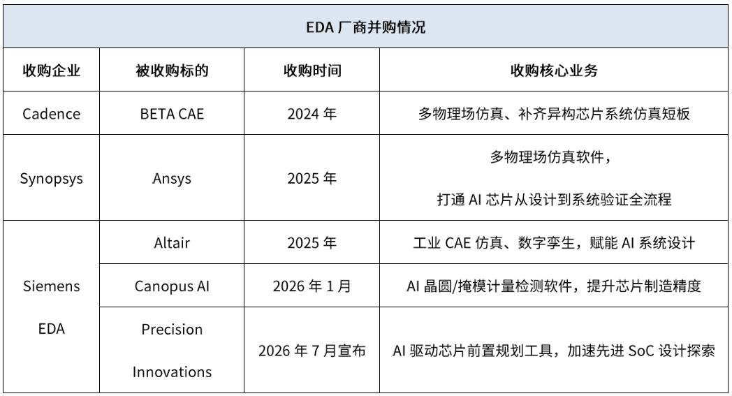
Source: Semiconductor Industry Observation statistics
This change in tool attributes and service boundaries precisely illustrates that the AI wave has brought two profound changes to the EDA industry: First, the market ceiling has been greatly raised, the EDA+simulation market size continues to expand, high-end AI computing chips are highly dependent on the integrated tool chain, and the discourse power of EDA tool manufacturers continues to increase, making EDA tools gradually change from a simple supporting role in the industrial chain in the past to a key link that can influence the AI chip design process and specifications. Second, industry concentration is further increasing, the comprehensive technical threshold required for AI chip development has been greatly raised, only leading manufacturers can fully meet the complete set of needs of computing power customers, and the living space of small and medium-sized single-tool enterprises in the high-end market is continuously squeezed.
At the same time, the AI industry has also driven EDA manufacturers to increase R&D investment in AI-native tools. While benefiting from the AI chip dividend, enterprises embed the capabilities of large models and AI agents into the whole process of design, verification, and layout optimization, so as to compress the R&D iteration cycle, optimize the chip PPA index, lower the threshold of chip design, and alleviate the constraint of insufficient supply of high-end chip engineers.
AI Rewrites the Logic of Chip Competition
Before the explosion of the AI industry, many chip manufacturers took a single chip as the core deliverable, and the focus of industry competition was concentrated on the parameters, power consumption and cost of the chip itself. However, as the generative AI market gradually divides into two major scenarios: cloud training and edge inference, for large computing power customers, procurement decisions no longer only measure chip indicators, but pay more attention to complete solutions such as hardware, scheduling software, and interconnection IP collaboration. Therefore, AI demand has also reconstructed the competition logic of the chip track. Reflected at the capital level, semiconductor chip manufacturers have invested in acquiring AI enterprises in the past two years, and these enterprises are clearly divided into the cloud computing power track and automotive and industrial edge scenarios.
In the cloud computing power track, AI inference demand has exploded intensively, and supply constraints of HBM memory and CoWoS advanced packaging have further amplified the supply shortcomings of traditional GPUs. NVIDIA adopts the model of technology licensing combined with core team absorption to integrate Groq's differentiated LPU inference architecture to avoid the capacity constraints of HBM and CoWoS; by acquiring Sched MD, it has mastered the Slurm open source scheduling system and improved the workload scheduling capability of large-scale AI clusters. AMD acquired dedicated inference chip manufacturer Taalas, combined with its original Xilinx adaptive computing power assets and SiloAI model software, to build a full-stack product system for the Helios rack. Both leading AI chip enterprises have supplemented their inference hardware and supporting software capabilities through mergers and acquisitions, breaking through the growth boundary of a single GPU and improving the structural contradiction of computing power supply.
In the edge track, AI capabilities continue to sink from the cloud to scenarios such as automobiles, robots, and industrial vision, forcing traditional industrial control and automotive chip manufacturers to supplement NPU and high-speed interconnection assets through mergers and acquisitions. NXP acquired Kinara's programmable NPU and Aviva Links' automotive high-speed SerDes to consolidate the hardware base of automotive multimodal large models; Microchip has signed an agreement to acquire low-power edge AI chip manufacturer Hailo to supplement the AI acceleration capability of embedded terminals; ON Semiconductor plans to acquire Synaptics to integrate perception, computing and wireless link assets and deploy Physical AI systems. The accelerated implementation of the AI industry has upgraded edge computing power from an additional product function to a core competitiveness. For traditional MCU manufacturers, if they cannot establish effective edge AI capabilities, it will be difficult for them to capture the incremental markets in the automotive and industrial fields.
In addition, in the analog and power sectors, Texas Instruments acquired Silicon Labs to strengthen its mixed-signal and wireless connectivity product matrix and ensure the product supply of edge AI devices; ON Semiconductor acquired Qorvo's SiC JFET business to improve the power supply supply chain for AI servers. The connection and energy supply demands of edge AI devices have further upgraded the importance of analog and power chips.
From cloud computing power to automotive and industrial edges, a series of intensive capital operations reflect that generative AI has reshaped the value distribution of the chip industry. The valuation of core assets such as dedicated inference architectures, high-speed interconnection IP, and AI cluster scheduling software has increased significantly, while traditional mature general-purpose chips are facing sluggish growth. The Matthew effect in the industry continues to strengthen, and enterprises that have both cloud-edge dual-track layout and software-hardware integration capabilities are more likely to obtain computing power orders.
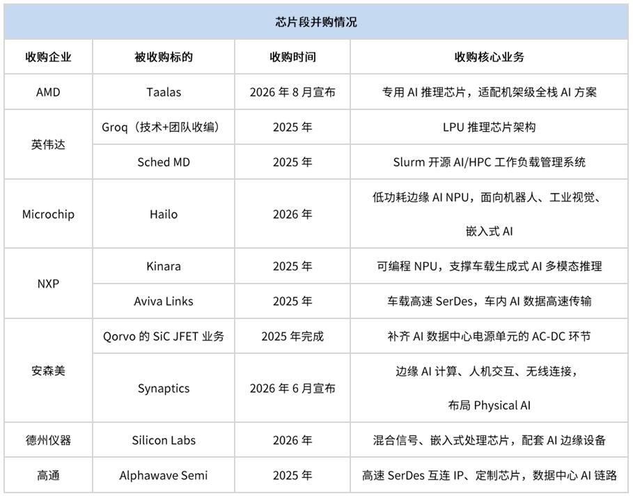
Source: Semiconductor Industry Observation statistics
Advanced Packaging Has Become a Strategic Resource
The explosion of computing power demand has also been transmitted to the back-end manufacturing link, making advanced packaging a strategic resource in the industrial chain. In the past division of labor in the industrial chain, wafer manufacturing and packaging & testing were long positioned as supporting links, and capacity allocation was prioritized for consumer electronics such as mobile phones and PCs. However, AI computing chips widely adopt 2.5D CoWoS and HBM stacking solutions, and the multi-layer stacking of HBM needs to cooperate with CoWoS packaging, making advanced packaging capacity the core bottleneck restricting GPU shipment. The industry has long been in a tight balance between supply and demand, which has completely rewritten the market's value judgment on manufacturing-side assets. Facing the tight situation, all parties have different response paths: memory manufacturers such as Samsung, SK Hynix, and Micros mainly expand HBM capacity by building their own factories; while wafer, packaging & testing, and equipment enterprises simultaneously adopt the mode of building new production lines and acquiring idle plants to quickly release supply and supplement the shortcomings of each link.
Specific to leading manufacturers, in the face of the phased capacity gap of CoWoS technology and supporting high-end substrates, TSMC not only builds a large number of new factories, but also acquires idle plants of Innolux in Tainan to quickly convert them into CoWoS capacity; ASE also increases capital expenditure to build new production lines while acquiring idle plants to expand advanced packaging capacity, so as to stabilize its own AI chip packaging and testing supply capacity; Applied Materials has completed the acquisition of the NEXX business under ASMPT to supplement the panel-level packaging deposition equipment required for mass production of large-size AI accelerators, filling the shortcomings of high-end chip manufacturing equipment.
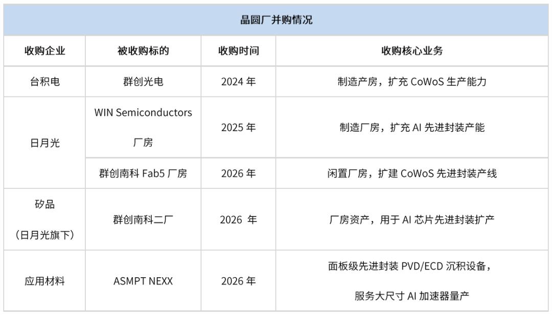
Source: Semiconductor Industry Observation statistics
Through a series of changes on the manufacturing side, we can see the profound impact of AI on the wafer manufacturing field. Advanced packaging is no longer just a back-end supporting process, but has become a core strategic asset that determines the upper limit of computing chip shipment. Manufacturers with their own plants and equipment have stronger bargaining power in the supply chain game; Secondly, the capacity pricing logic has switched. In the past, the foundry segment mainly competed by cost, while current customers are willing to pay a premium for long-term stable advanced packaging capacity, and acquiring physical plants has also become an important means to lock in supply; Third, vertical integration has become an important development direction in the computing power track. IDMs and leading packaging & testing enterprises get through the links of wafer, packaging and power devices through mergers and acquisitions, so as to reduce the uncertainty of AI chip delivery.
What Does the Intensive M&A Imply
The current cross-link intensive M&A in the semiconductor industrial chain is not a conventional commercial behavior, but a concentrated manifestation of AI computing power reshaping the industry pattern, marking that the semiconductor industry has entered an irreversible structural transformation cycle. According to Gartner's forecast, AI semiconductor revenue will account for more than 30% of the whole industry in 2026, and the computing power track has officially become the core growth engine of the industry. Compared with the rapid expansion of the computing power sector, the growth momentum of traditional consumer electronics such as smartphones and PCs and industrial control chips continues to weaken, and industry R&D investment, capital expenditure and M&A resources continue to tilt towards AI computing power. The computing power demand of large models has dominated the new round of the semiconductor industry cycle.
Under this industrial background, M&A has become a core means for enterprises to quickly adapt to AI changes, bringing significant positive value to industry development. Through the rapid integration of technology, teams and assets, enterprises can greatly shorten the cycle of full-stack AI technology layout and avoid the uncertainty of long-term independent R&D; at the same time, industrial-level capital integration effectively reduces redundant R&D investment in the industry, accelerates the implementation of generative AI technology in physical scenarios such as automobiles and industry, and promotes the rapid maturity of the intelligent computing power industry. In addition, the lightweight technology acquisition model can adapt to the increasingly strict anti-monopoly regulatory environment around the world, providing a flexible and efficient path for enterprises to supplement cutting-edge technologies and improve their full-stack product system.
However, the full-track and high-frequency intensive M&A has also laid long-term structural hidden dangers for the industry. On the one hand, core strategic resources such as EDA tools, cloud computing power, and advanced packaging continue to gather to leading giants, industry concentration is constantly increasing, and the living space of small and medium-sized chip design and tool R&D start-ups is continuously squeezed, which weakens the diversified innovation vitality at the bottom of the industry. On the other hand, post-merger integration problems are common. The technical architecture and R&D system of start-up teams are not sufficiently compatible with the original business model of large manufacturers, which easily leads to problems such as core talent loss, technology implementation failing to meet expectations, and advanced architectures being difficult to scale for commercial use, greatly reducing the M&A value. At the same time, cross-border M&A continues to face the uncertainty of geopolitics and multi-country anti-monopoly reviews, and risks such as transaction termination and pre-cost loss are prominent.
From the perspective of long-term industrial development, M&A is only a short-term tool for enterprises to quickly supplement their capabilities, and cannot replace the core competitiveness built by independent R&D, organizational collaboration and commercial operation. The AI transformation of the semiconductor industry ultimately does not compete on the quantity and scale of M&A targets, but on whether enterprises can get through the full chain resources of chip design, hardware computing power and advanced manufacturing, and realize the in-depth integration and long-term implementation of technology, team and production capacity.
Final Notes
Combined with forecasts from a number of analytical institutions, the AI-driven semiconductor integration cycle will last at least until 2030. This means that the current wave of M&A may only be the prelude. When computing power defines chips and chips define everything, the competition in the semiconductor industry has been upgraded from "selling chips" to an architecture-level competition that "defines the next generation of computing infrastructure". In this competition, no one can rely on past leading advantages to rest on their laurels. Whoever can see the direction of the AI era clearly will laugh last. The semiconductor industry has never been as fanatical and cruel as it is today.
This article is from the WeChat official account "Semiconductor Industry Observation" (ID: icbank), author: Xia Xue, published with authorization from 36Kr.