Advancing towards the 0.2nm process
As logic process scaling enters the angstrom era, vertical-stacked complementary field-effect transistors (CFETs) based on atomically ultra-thin two-dimensional (2D) semiconductors provide a potential path for device scaling to break through the A2 node. This paper constructs an integrated process flow targeting the A2 node with a contact polycrystalline silicon pitch (CPP) of 36 nm and a gate length (Lg) of 10 nm, and conducts preliminary verification on several key process modules. Although 2D gate-all-around (GAA) CFETs adopt atomically ultra-thin channels, their scaling advantage in contact polycrystalline silicon pitch under the A2 node is not superior to that of silicon-based GAA CFETs, because the constraints of contact formation make the minimum CPP of both around 36 nm.
In addition, this paper combines key evaluations with a multi-scale power-performance-area (PPA) evaluation framework, which covers quantum transport simulation, compact model generation, definition of 2D CFET GAA integrated process flow for the A2 node, parasitic parameter extraction, and circuit-level benchmark testing. The analysis results show that the expected performance advantages of 2D GAA CFETs are severely restricted by non-ideal effects, especially high contact resistance and dominant layout parasitic capacitance.
Although architectural optimization can improve the capacitance-resistance ratio, the corresponding increase in absolute capacitance will limit the performance improvement at the circuit level. To achieve substantial breakthroughs, collaborative optimization of contact structures, transport characteristics and parasitic parameters is required, and new CFET architectures adapted to 2D materials need to be developed at the same time.
Introduction
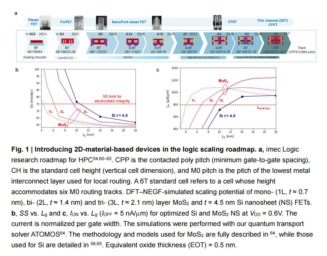
With the rise of data-intensive workloads in the fields of artificial intelligence (AI) and high-performance computing (HPC), global computing demand is still soaring sharply despite the limited power consumption budget. To sustain this growth, continuous advancement in transistor scaling technology and brand-new design innovations are required to improve performance per watt. As shown in Figure 1a, the significant scaling technology of silicon transistors has brought exponential performance improvements: planar metal-oxide-semiconductor field-effect transistors (MOSFETs) have been replaced by fin field-effect transistors (FinFETs), and in recent years they have been replaced by gate-all-around (GAA) nanosheet field-effect transistors, pushing the logic device process into the single-digit nanometer range. Today, as the industry enters technology nodes often called the "angstrom era" — where critical feature sizes are close to atomic-scale dimensions — traditional scaling technologies are stagnating.
Advanced GAA transistors have achieved gate lengths close to 10nm with excellent electrostatic control capability. For example, IBM's research alliance successfully demonstrated stacked nanosheet field-effect transistors with a gate length of about 12nm by thinning the silicon channel to about 5nm. However, scaling the gate length far below about 10nm in silicon-based materials requires reducing the channel thickness to 3nm, which brings severe challenges such as enhanced quantum tunneling effect and reduced carrier mobility. In addition, continuous size compression severely limits the effective channel width (Wch) available for each transistor, because the substantial reduction in standard cell height will inevitably limit the total width that can be allocated to each device. This width reduction reduces the drive current per transistor and exacerbates the parasitic capacitance per unit channel width. Taken together, simply reducing the size of silicon transistors can no longer guarantee significant improvements in circuit speed or energy efficiency.
If traditional scaling processes hit a bottleneck, what is the next step for development? One approach that is being explored in depth is to adopt new channel materials and 3D integration schemes to improve CMOS performance. Two-dimensional (2D) semiconductors are at the forefront of this exploration. Atomically thin 2D materials (such as monolayer MoS₂, WSe₂) can be used as transistor channels that are only a few atoms thick. Their extremely thin characteristics provide unprecedented electrostatic control capability, enabling robust switching performance even when the gate length is only a few nanometers. Figures 1b and c examine the scaling potential by comparing monolayer (1L, t≈0.7nm), bilayer (2L, t≈1.4nm) and trilayer (3L, t≈2.1nm) MoS₂, as well as t=4.5nm silicon nanosheet (NS) field-effect transistors (FETs), focusing on subthreshold swing (SS) and drive performance (ION under fixed IOFF and VDD conditions). By reducing the t value, electrostatic integrity (SS, Figure 1b) is maintained at lower Lg. This means that as Lg scales, ION (under fixed IOFF and VDD conditions, Figure 1c) is significantly improved. Therefore, 1L-MoS₂ has the best scaling potential, and can still maintain the target transistor current required for logic operation when Lg≈4nm, while Si NS with t=4.5nm can only be scaled to Lg≈12nm.
It is hoped that 2D materials can open up new scaling paths, especially when combined with vertical integration. For example, monolithic complementary field-effect transistors (CFETs) — where p-type FETs and n-type FETs share the same footprint in a vertical stack — can double transistor density without shrinking horizontal feature sizes. If 2D semiconductors are introduced into such GAA CFET structures as channel materials, it may be possible to simultaneously achieve the ultimate gate length scaling and extremely high device density. This vision has inspired a large number of studies: early experiments have demonstrated that 2D GAA transistors have near-ideal subthreshold behavior, and even the first batch of 2D CFET prototypes have emerged, and this research direction has received widespread global attention.
However, a realistic assessment of the prospects of 2D CFETs must acknowledge two limiting factors.
First, silicon materials are not yet obsolete. Intel recently demonstrated GAA "ribbon" transistors with physical gate lengths less than 10nm (achieved by adopting an ultra-thin silicon ribbon channel of about 2nm) — which shows that despite the significant increase in process complexity, silicon devices can still be pushed to such extreme levels. In fact, industry roadmaps (such as the imec roadmap in Figure 1a) predict that even if 2D channels are eventually adopted, it will only happen after silicon CFET technology is fully exhausted — that is, beyond the last all-silicon CFET process node (after approximately A2). In other words, 2D materials are regarded as a potential next step after pushing silicon technology to its limits, rather than an immediately available alternative.
Second, 2D CFETs face significant integration and design challenges. Wafer-scale growth or transfer of high-quality monolayer films, their reliable integration into complex 3D device stacks, and the achievement of ultra-low contact resistance without doping are still unsolved research problems. In addition, even if these obstacles are overcome, we must also consider whether the traditional GAA CFET architecture, which has been carefully optimized for silicon materials, is also applicable to 2D channels. The current key question is: can integrating 2D channels using the industry mainstream gate-all-around CFET architecture at the A2 node and more advanced process nodes bring the expected improvements in performance, power consumption and area?
Starting from these challenges, this paper conducts a critical assessment of the potential of 2D CFETs. First, by proposing a sequential CFET integration scheme, we explore under what circumstances and how 2D channels can be practically introduced beyond the final node of silicon-based CFET (A2). Then, we review the latest progress of GAA nanosheet transistors, and point out which aspects require new solutions due to scaling pressure compared with silicon technology. Next, based on these structures, we conduct a power-performance-area (PPA) analysis of promising 2D GAA/CFET devices to evaluate whether they can meet the iso-frequency scaling target of the A2 node.
Stepwise 2D CFET integration process for A2 node and more advanced process nodes
Figure 2 shows the process flow of 2D channel CFET with GAA architecture targeting the target A2 process node, contact polycrystalline pitch (CPP) = 36nm and gate length (Lg) = 10nm. This process adopts a full sequential CFET integration process, which enables independent manufacturing of top and bottom devices. In contrast, monolithic CFET integration requires top and bottom devices to share multiple process steps. One of the key reasons for adopting sequential integration is to simplify the deposition bottleneck in the atomic layer deposition (ALD) process — in the common replacement metal gate (RMG) process of monolithic CFET, high-k materials and gate work function metal (WFM) need to completely wrap around the channel. When Lg=10nm, the vertical channel gap is about 5–7nm. In the conventional RMG process, after completing the high-k material and gate WFM deposition of the first device, the vertical gap may be squeezed closed, resulting in impossible or only limited WFM patterning and/or WFM deposition for the second device. Since the top and bottom RMG modules can be processed independently, sequential CFET integration effectively alleviates this bottleneck. Compared with monolithic CFET, full sequential CFET also has other general process simplification advantages, including lower aspect ratio etching and deposition.
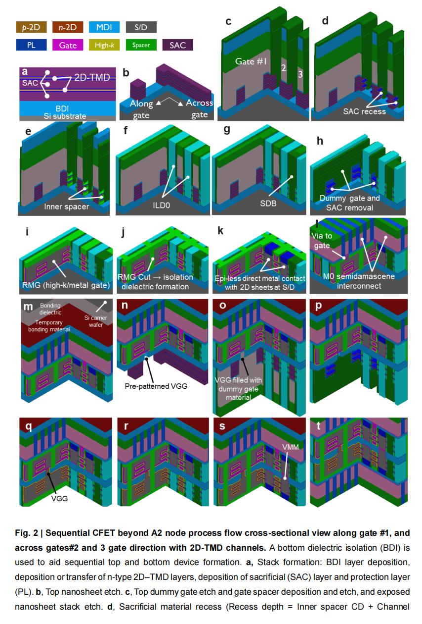
This sequential process flow first forms the top NMOS device stack (Figure 2a), which includes two 2D channels (such as MoS₂), a thin protective layer (PL) wrapping the channels, a sacrificial layer (SAC), and a bottom dielectric isolation (BDI) layer. The key manufacturing steps include nanosheet etching, dummy gate formation, internal interlayer dielectric formation, SAC removal, NMOS RMG, RMG cutting, source/drain (S/D) contact formation, and front-end back-end-of-line (BEOL) formation (Figures 2b–m). After the NMOS device is completed, the wafer is bonded to the carrier wafer, flipped, and thinned from the substrate until the BDI layer is reached. Subsequently, the bottom PMOS device is formed in a similar sequence. Then the bottom PMOS stack is formed above the BDI layer (Figure 2n), which includes the PMOS 2D channel (such as WSe₂), followed by PMOS RMG integration (Figure 2q).
Sequential CFET integration also provides the possibility to easily manufacture inter-gate vias (VGG). This provides CFET with a wiring option from top gate to bottom gate, that is, a split gate function, which is a scaling accelerator at the standard cell library level. In monolithic CFET, the VGG process is more complex and requires more and more complex process steps. Here, the BDI layer is also utilized by performing VGG patterning and metallization within the BDI layer. The BDI layer not only ensures high uniformity of VGG within the wafer, but also provides vertical edge placement error (VEPE) margin to maintain the isolation distance between the top gate and the bottom gate.
By using two-dimensional transition metal dichalcogenide (TMD) nanosheets instead of silicon nanosheets, this process flow is significantly simplified. We assume that the 2D TMD RMG process does not require the high-temperature (T>800℃) reliability annealing usually adopted in silicon RMG processes. Similarly, other annealing processes with temperatures higher than 400℃ on the A2 node, such as interlayer dielectric zero (ILD0) densification annealing, can also be omitted. This makes the 2D CFET front-end-of-line (FEOL) process flow compatible with a typical copper-based back-end-of-line (BEOL) stack. Therefore, for 2D-CFET, we can adopt a simpler and fully sequential process flow that only requires one wafer flip: top RMG → top S/D contact → front-side BEOL → wafer flip → bottom RMG → bottom S/D contact → back-side BEOL. It should be noted that since the front-side BEOL is compatible with the BEOL stack of the bottom RMG and other processes, the front-side BEOL can be exposed to the bottom RMG and other processes. However, the sequential silicon CFET process flow requires two wafer flips to prevent the back-end process from being exposed to high temperatures during the RMG process. The specific process is as follows: top RMG → wafer flip 1 → bottom RMG → bottom source/drain contact → back-side BEOL → wafer flip → top source/drain → front-side BEOL.
The 2D GAA process flow also differs from the Si GAA process flow in the source/drain (S/D) contact module. In the proposed 2D process flow, source/drain contacts are formed by direct metallization on the exposed 2D flakes (Figures 2k, s). This is different from the Si GAA process flow, in which doped Si or SiGe is selectively epitaxially grown from the exposed silicon wafers. Section 4 discusses in detail the differences in S/D contact formation methods between 2D and Si processes, as well as related contact resistance and scaling challenges.
Finally, RMG cutting is performed to isolate different devices. In the proposed sequential CFET process flow, RMG cutting of the top and bottom devices is performed independently, which means that the etching depth of RMG cutting can be reduced. When the maximum etching aspect ratio is fixed, the reduced etching depth helps to reduce the CD value of RMG cutting, which determines the gate line tip-to-tip (t2t) distance. This in turn allows the nanosheet channel width to be increased at the same cell height, thereby improving device performance. The two potential disadvantages of independent RMG cutting are: the separation of the upper and lower RMG cutting lithography processes will introduce additional overlay errors; and the need to additionally use expensive high numerical aperture (high NA) gate cutting masks, which increases the overall cost. Therefore, for cases where the gate t2t requirement is looser, a common RMG cutting process with a single mask can be considered. Both scenarios (common RMG cutting and independent RMG cutting) will be considered in the PPA evaluation in Section 5.
Latest Progress: Development Status of 2D CFET
Experimental two-dimensional field-effect transistor (2D FET) prototypes are developing rapidly, but there is still a big gap from the process flow outlined in Section 2. Figure 3a summarizes the increasing complexity of these device architectures, from single-gate (SG) tungsten disulfide (WS₂) field-effect transistors fabricated in the imec fab, to dual-gate (DG) structures with improved electrostatic control performance. The third transmission electron microscope (TEM) image in Figure 3a shows a more advanced 2D GAA structure, in which a high-k (high κ) dielectric layer and a metal gate completely wrap the monolayer channel. Finally, vertically stacked 2D nanosheets prepared by a single-step gate stack deposition process have also been verified. This structure is an important predecessor of the CFET integration process flow outlined in Section 2 at the device level.
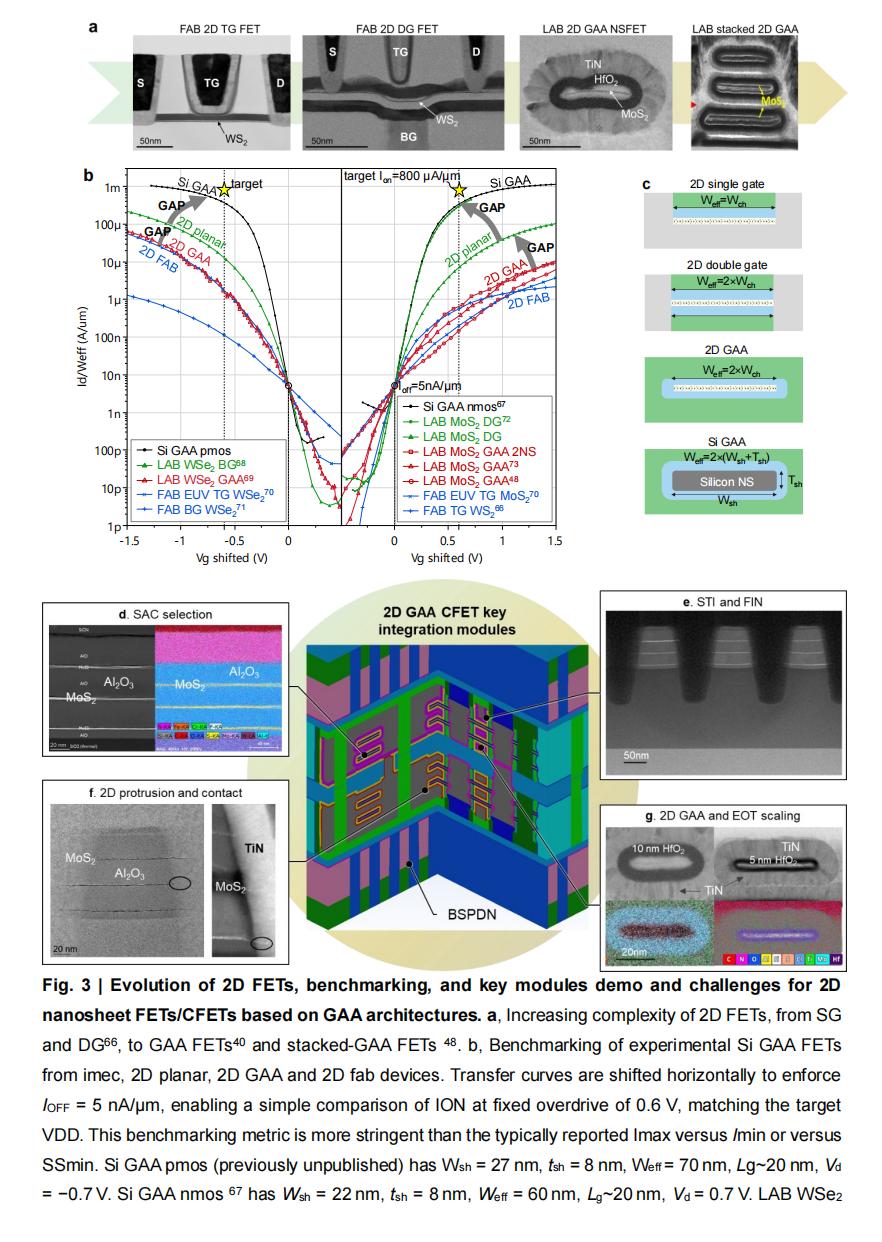
Although the evolution process from planar single-gate (SG) to dual-gate (DG), then to gate-all-around (GAA) and stacked GAA is very similar to the historical evolution of silicon transistors, it is expected that this evolution will not bring similar performance advantages to two-dimensional field-effect transistors (2D FETs). Although the transition from single-gate (SG) to dual-gate (DG) improves both electrostatic control and drive current, the transition to gate-all-around (GAA) is not expected to further increase on-current or improve electrostatic control because the channel is only one monolayer thick. On the contrary, the transition from DG to GAA is driven by the integration process outlined in Section 2, where the gate module is applied to all nanosheets simultaneously.
Experiments show that compared with the most advanced SG or DG planar MoS₂ and WSe₂ laboratory devices, GAA 2D field-effect transistors have a performance gap due to increased integration complexity. This is evident from the electrical benchmarks in Figure 3b: 2D GAA FETs perform worse in terms of SS and drive current compared to planar laboratory devices. This benchmark considers various cases with Lch=20–100nm, and as shown in Figure 3c, the drive current is normalized by the effective width (Weff) to ensure a fair comparison of different gate geometries. Importantly, this performance loss is not inherent to the GAA structure, but stems from the greater difficulty in forming the gate stack and the generally higher contact resistance in experimentally implemented GAA devices. In addition, atomically thin channels are extremely sensitive to metal deposition, stress and process-induced damage.
A similar trend has been observed in planar two-dimensional field-effect transistors (2D FETs) fabricated in imec's fab, although benefiting from improved process control in the fab, their performance is still inferior to lab-scale planar 2D FETs. This is mainly due to the more stringent restrictions on available materials and processes in the fab.
Specifically, although titanium, tungsten