SerDes has become the make-or-break factor.
In the past few years when the large model wave has swept across the globe, the computing power architecture of data centers has been iterating rapidly. From the early stage of stacking general-purpose GPUs to the current stage where major cloud vendors have stepped in to develop custom ASICs, the arms race on the computing power side has entered a new phase. What many people have not noticed is that the more fiercely the computing power cores compete, the more easily data transmission between chips becomes a bottleneck. The high-speed interconnection technology hidden at the bottom of chips is evolving from a supporting component to a core capability.
In June 2025, Qualcomm announced the acquisition of Alphawave Semi, the world's leading high-speed connection IP vendor, for approximately 2.4 billion US dollars, to reinforce its core technical reserves of SerDes high-speed interfaces and UCIe die-to-die interconnection, and simultaneously incorporate Open-Silicon's full custom ASIC design business under its banner. At the end of July 2026, MediaTek CEO Richard Lai revealed at a financial presentation that the development of 400G/448G SerDes IP is progressing smoothly, and the full set of standardized IP resources will complete all verification and be delivered to customers in the second half of 2027 to support the hardware development of next-generation cloud custom ASICs.
The two enterprises that originally focused on consumer chips have simultaneously increased their investment in SerDes, which represents a shift in the underlying logic of the computing power hardware track. According to statistics from PW Consulting, the global SerDes IP core market reached 1.41 billion US dollars in 2025. Divided by end users, data center and cloud computing scenarios account for 49.9% of the total. It is estimated that by 2032, the market size will reach 3.35 billion US dollars, with a projected compound annual growth rate of 13.15%.
As the SerDes interface becomes the core of high-speed connections, chip designers are increasingly relying on mature SerDes IP to reduce integration risks and shorten time-to-market. In the past, the industry competed on chip computing performance, but now high-speed interconnection PHY IP has become the core bargaining chip for winning custom ASIC orders from cloud vendors.
Why ASICs Must Compete on SerDes
To handle specific artificial intelligence training and inference workloads, cloud service and AI providers such as Google, Amazon Web Services, Microsoft, OpenAI, and Apple are accelerating the deployment of servers with AI ASICs, and custom computing chips are entering a large-scale implementation cycle.
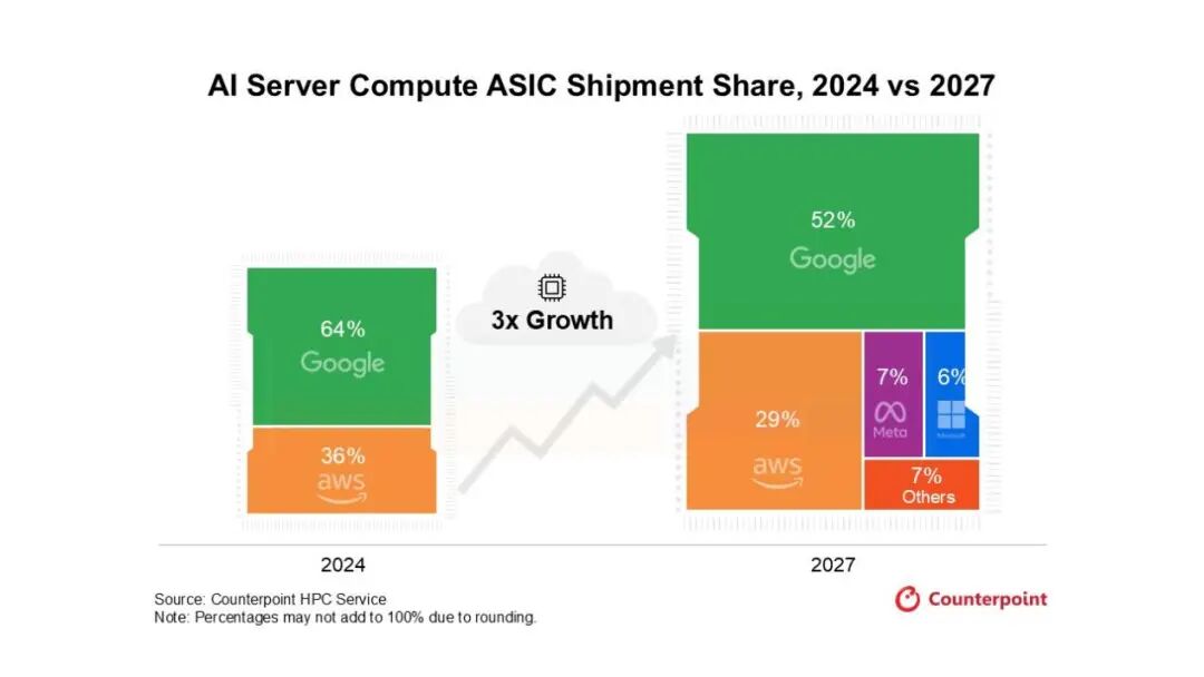
Comparison of AI ASIC shipment share in 2024 and 2027 Source: Counterpoint
Counterpoint estimates that the CAGR of the global AI ASIC market from 2024 to 2027 will be 34%, and the overall shipment volume in 2027 will be three times that of 2024. JPMorgan Chase further predicts that the ASIC shipment volume in 2026 is expected to be 6.8 million units, and the GPU shipment volume will be 9.5 million units. Among the global AI chip shipments, ASICs account for about 42%. But by 2027, the ASIC shipment volume is expected to reach 12.5 million units, accounting for 53%, surpassing GPUs for the first time and becoming the mainstream acceleration hardware. The self-developed dedicated chips of cloud vendors such as Google, Amazon, and Meta continue to be delivered in large volumes. The custom architecture can eliminate redundant circuits, with significant long-term TCO advantages. At the same time, switch chips also highly rely on SerDes. Data from Growth Market Reports shows that the CAGR of the global high-speed SerDes overall market from 2025 to 2034 is 13.1%, and data center switching equipment is the core source of demand, which is also the underlying motivation for Broadcom to continue to deeply cultivate this track for many years.
During the operation of large-scale computing power clusters, the contradiction between redundant computing power and transmission bottlenecks continues to become prominent. ODCC published measured data in the White Paper on Next-Generation Intelligent Computing DC High-Speed Interconnection 448G/lane Demand, showing that in the large model training scenario with trillion-level parameters, the communication overhead generated by data interaction accounts for more than 70% of the total operating cost, and a large amount of computing power resources are idle due to data congestion.
To understand why SerDes is so important, you first need to figure out what it actually is. SerDes is short for Serializer and Deserializer, whose core function is to perform serial-parallel conversion. The transmitting end converts parallel data into high-speed serial signals for transmission, and the receiving end converts them back. It sounds that the principle is not complicated, but after the rate reaches the level of 224G and 448G, the difficulty will rise exponentially. When signals travel on PCBs, cables, and package substrates, they will attenuate, suffer crosstalk and noise, and these problems will become more serious as the rate increases. Early low-speed SerDes used NRZ modulation, where one symbol transmits 1 bit; after 112G, PAM4 is widely adopted, where one symbol transmits 2 bits, and the spectrum is compressed by increasing the modulation order. Moving towards 448G, the industry is also exploring PAM6 or even PAM8, where one symbol can transmit more bits, but the requirement for signal signal-to-noise ratio is also more stringent.
Another core reason why high-speed SerDes is difficult to develop is that it is a typical digital-analog hybrid circuit. Digital logic can continuously reduce the area with advanced processes, but the performance of analog circuits is highly related to processes, layout design, and signal integrity. Even for 224G SerDes, the power consumption, yield, and signal quality made by different teams may differ significantly. This is why high-end SerDes IP is highly concentrated in a few companies, with very high talent barriers, and it cannot be quickly developed just by investing money.
The high technical difficulty corresponds to great industrial weight. As the serial transmission channel between chips, the rate iteration of SerDes can simultaneously reduce the number of wiring and lower the energy consumption of the whole machine. OIF industry estimates show that the SerDes circuit in high-end switching chips accounts for more than 40% of the total power consumption; in the scenario of high-density Chiplet integration, the local heat flux density can reach 50W/cm², and the energy efficiency performance of interconnection circuits directly determines the cabinet deployment cost, which is also the priority assessment indicator for cloud vendors to evaluate hardware solutions.
Therefore, for all vendors that lay out custom ASICs, independent and controllable high-speed SerDes is a core asset that cannot be bypassed. The upper limit of computing power of a single chip is determined by the computing unit, but the overall throughput efficiency of a cluster with tens of thousands of cards is completely constrained by the interconnection link. The main battlefield of computing power competition has shifted from single-core performance to the global interconnection scheduling capability.
Who is Using SerDes to Develop ASICs
Market demand and technical value have fully confirmed the strategic status of SerDes, and at the same time, leading chip vendors at home and abroad have taken completely different positioning paths.
In the track of data center high-speed interconnection, Broadcom is a well-established veteran player. It has developed from the era of switching chips, and Broadcom has been developing SerDes for longer than the establishment time of many AI chip companies. It is also a core participant in the formulation of the OIF CEI-448G standard, with heavy discourse power. At present, Broadcom has launched a 448G SerDes PHY prototype, which is compatible with both PAM4 and PAM6 technical routes, allowing it to both attack and defend. Relying on this mature interconnection technology, Broadcom has long won custom ASIC orders from leading cloud vendors such as Google, and is a recognized leader in the track. According to Counterpoint's forecast, Broadcom will maintain its leading position as a top AI ASIC design partner by 2027.
As one of Broadcom's customers, Meta is quite special. Its MTIA chip is fully architected and independently developed by Meta, instead of directly purchasing off-the-shelf ASIC chips from Broadcom. However, the two sides have established a long-term joint R&D cooperation, and Broadcom will provide underlying physical layer technical solutions such as high-speed SerDes, Ethernet interconnection, and advanced packaging for MTIA.
Marvell has also been deeply engaged in data centers for many years, and is one of the traditional main vendors. The enterprise independently develops the full set of SerDes technology, and simultaneously launches the full custom ASIC business, which has long been bound to the stable demand of cloud vendors such as AWS, with a steady and down-to-earth development rhythm.
Intel adopts the IDM full-stack self-developed route, independently completes the development of 112G/224G high-speed SerDes, and adapts to the UCIe chiplet interconnection standard at the same time. The technology is supplied to its own AI acceleration ASIC and data center switching ASIC. Its Gaudi series AI computing chips have built-in self-developed Die-to-Die SerDes, realizing multi-card cluster interconnection relying on on-chip integrated 100G Ethernet channels, and simultaneously laying out silicon photonic CPO and 448G interconnection prototypes, providing a full set of computing power ASIC solutions for government, enterprise and cloud vendors.
MediaTek is a new competitor that crosses from the consumer electronics industry to the computing power track, and gradually makes up for its high-speed interconnection capability through ten years of long-term independent R&D. Its high-speed IO team can be traced back to PowerRise Communications established in 2015, which was merged into the parent company in 2019 and specifically focuses on the data center direction, developing all the way from low rate to mass production of 224G, and now sprinting to 336G and 448G. There are industry rumors that MediaTek's 336G solution is expected to enter Google's next-generation TPU supply chain, but neither side has officially confirmed it for the time being. But what really deserves attention is the 448G SerDes IP that will be launched in 2027, which will be the core bargaining chip for MediaTek to compete head-on with Broadcom.
Qualcomm quickly enters the market through capital mergers and acquisitions, with a more direct playing style of exchanging money for time to achieve one-step completion through acquisition. The $2.4 billion acquisition of Alphawave is equivalent to quickly incorporating more than ten years of technical accumulation of others into its own system. What it obtains is not only the DSP architecture SerDes PHY, but also the UCIe die-to-die interconnection IP and Open-Silicon's custom ASIC business. This set of assets is very flexible in use: internally, it can support its own server CPUs and AI accelerators, completing the full chain from computing to transmission; externally, it can continue to provide IP licensing and custom design services, and one acquisition supports two business growth paths.
Nvidia adheres to a completely closed self-developed route, its NVLink interconnection protocol is completely self-developed for its own use, the Rubin platform has achieved 400G NVLink, and it is still evaluating the 448G solution. But this set of technology only serves its own GPU clusters, does not sell IP externally and does not take external ASIC orders, representing the unique idea of end computing power giants to control core interconnection technology.
In addition to the whole machine chip enterprises that develop ASICs by themselves, there are two types of indispensable supporting players in the track that do not directly deliver complete ASICs. One type is IP vendors originating from EDA giants, represented by Synopsys and Cadence. They do not make finished chips, and specifically license SerDes PHY IP to downstream chip design companies, which are technical suppliers for many small and medium-sized ASIC vendors. Relying on the ecological binding of EDA tools, the two companies have a very high market share in the SerDes IP market, covering the full spectrum of products from low rate to 112G and 224G, and 448G is also being promoted synchronously.
The other type is independent chip vendors focusing on high-speed interconnection, and Credo Technology is a typical representative. It does not develop complete AI ASICs, focuses on the R&D of high-speed SerDes, DSP and Retimer chips, and provides supporting components for data center switches and AI accelerators. After the outbreak of AI computing power, the demand for cluster interconnection continues to skyrocket, and this type of enterprise that deeply focuses on vertical interconnection hardware has obtained significant market dividends, with revenue growth rate leading the industry average level.
Industrial Changes and Implementation Challenges Brought by 448G
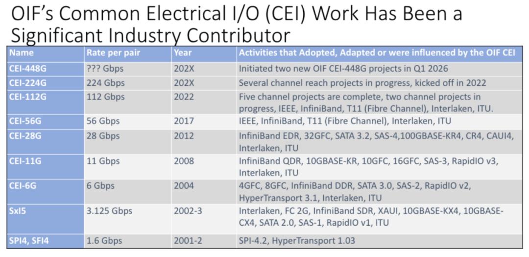
The positioning of various vendors in the SerDes track is essentially to make advance layout for the next-generation technology node. At present, 224G has entered the large-scale commercial stage, and the next recognized technical inflection point in the industry is 448G. This generation of rate upgrade is not just a doubling in numbers, but will directly rewrite the access rules and competition pattern of the ASIC market.
Source: OIF
From the perspective of global standards and the demand of leading enterprises, 448G will become the access threshold for next-generation ASICs. OIF launched the CEI-448G framework project in 2024, and released the complete specification in November 2025, dividing four transmission distance standards to support the iteration of 1.6T and 3.2T Ethernet in the future. LightCounting research shows that hyperscale vendors such as Google and Meta have clearly stated at the OCP Summit that the new generation of computing power hardware will take 448G interconnection as the basic hardware indicator.
Only the rate is not enough. After 448G is implemented, the dimensions of industry competition will also rise to a higher level. The differentiation space for single chip performance is getting smaller and smaller. What really makes the gap between vendors is whether they can package SerDes, die-to-die interconnection, advanced packaging, and CPO into a complete pre-verified subsystem. MediaTek cooperates with TSMC's COUPE platform for integrated verification, and Broadcom lays out both silicon photonics and VCSEL co-packaging solutions, which essentially aim at system-level delivery capability. OIF estimates that 448G combined with CPO architecture can reduce the energy consumption per bit by 70%, which is also the core driving force for all parties to compete for full-stack integration.
While the competition dimension is upgraded, the long-term solidified market pattern will also be loosened. In the past, Broadcom dominated the market, and this round of 448G technology iteration is equivalent to reshuffling the cards. JPMorgan Chase predicts that after the 448G supporting ASICs are delivered in large volumes from 2028 to 2029, the track will shift from oligopoly to coexistence of multiple strong players. In addition, cloud vendors generally implement a dual-supplier strategy, so second-tier players such as MediaTek and Qualcomm all have the opportunity to share the incremental market.
The changes in the overseas market pattern also provide a clear reference sample for the domestic industry. Dataintelo's 2025 report shows that in the high-speed SerDes IP market in 2025, the top three players Synopsys, Cadence and Alphawave together account for 72.3%, and the overseas monopoly pattern is very obvious. Domestic vendors have only achieved large-scale commercial use at 56G and 112G at present. Therefore, MediaTek's playing style of long-term heavy investment, binding advanced processes, and full-chain collaboration is worthy of reference for domestic IP and ASIC enterprises.
After talking about the opportunities, we also need to look at the practical constraints. Although the prospect of 448G is clear, there are still many hard nuts to crack on the way to large-scale implementation. The first priority is process and production capacity. 448G is a high-frequency mixed-signal circuit, which highly relies on the top 2nm process. The complete tape-out and interoperation verification cycle is very long. Once the R&D is delayed, it will directly miss the bidding window of cloud vendors. In addition, the supply and demand of 2nm wafers and CoWoS advanced packaging have been tight for a long time. The industry generally estimates that the full set of 448G supporting hardware can be delivered in large volumes no earlier than 2028.
In addition to hardware production capacity, the uncertainty at the standard level cannot be ignored. At present, there are two parallel modulation routes in the industry: PAM4 and PAM6/PAM8. Chip vendors prefer mature and stable PAM4