chip, turning point
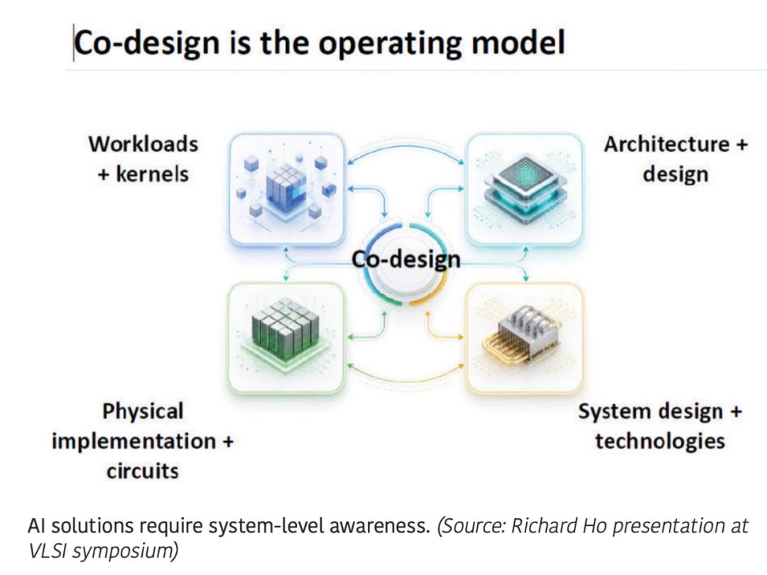
Although the shrinking of transistor dimensions is far from over, attendees of the 2026 Symposium on VLSI Technology and Circuits are urged to think more broadly at the system level. Richard Ho, Head of Hardware at OpenAI, called for a shift in mindset at the opening ceremony of the conference.
"Progress cannot be achieved solely by shrinking transistor dimensions; it also requires breakthroughs in circuits and technologies, such as memory integration, low-power interconnection, power delivery, heat dissipation, and advanced packaging," Ho said in his keynote speech.
Innovation in all fields must be collaboratively optimized within a coherent system architecture. "Only through holistic system-level innovation supported by rigorous execution can we achieve the required improvements in energy efficiency ratio and total cost of ownership ratio, so that the benefits of artificial intelligence can reach a broader group of people," Ho said.
The three pillars of AI hardware systems — computing, memory, and interconnection — cannot be viewed in isolation, and their interactions should be considered at the system level. This requires co-design of models and hardware to "match workload characteristics with architectural choices and technical capabilities".
"The development of AI hardware in the next decade will be defined by system-level innovation," Ho said.
CFET in the Post-Nanometer Era
In the short course speech on Monday, Guo from IBM Research outlined a roadmap that will lead the industry "all the way to 2040 to achieve transistor innovation".
After 12 years of FinFET development, the transition to Gate-All-Around (GAA or Nanosheet) is well underway, which has significant advantages in channel width flexibility, short-channel effects, and new innovation opportunities. After several generations of GAA devices, the focus will shift to stacked complementary field-effect transistors (CFET), commonly known as CFET, where two wafers are bonded together and optimized for crystal orientation. Guo said these complementary FETs will emerge in the post-1nm era, with device sizes reaching 2 angstroms.
For interconnections, cobalt or ruthenium (Co or Ru) liners are required, and copper reflow technology will bring larger copper grain sizes, thereby reducing resistance at 20nm pitch (10nm line width and 10nm space). Air gaps will also play a role.
"Beyond the 20nm pitch, we need new interconnection technology innovations. The I/O of stacked devices is also a major challenge, and we need innovations in DTCO (Design Technology Co-Optimization)," Guo said.
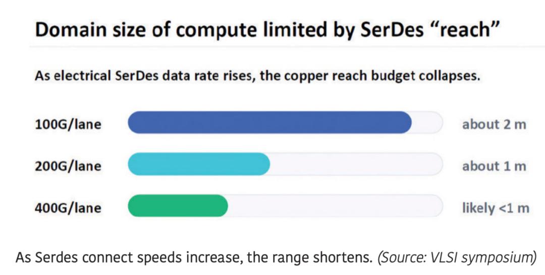
He said that some 1.4nm process designs require High-NA (High Numerical Aperture) lithography technology, while "1nm process designs absolutely require it", with advantages including improved line edge roughness (LER) and reduced variability.
Dwaipayan Biswas, Program Director at imec, analyzed the development prospects of artificial intelligence from a macro perspective. Citing a Google study, he pointed out that AI will have a wide range of application fields, and each field requires "specialized technical solutions".
In the next five to ten years, to meet these diverse market demands, heterogeneous 3D integrated circuits will continue to emerge, and chip-to-wafer and wafer-to-wafer hybrid bonding technologies will be more widely adopted. This fine-pitch 3D stacking technology is currently in progress and brings new opportunities. "We can use it to achieve architectural flexibility," Biswas said.
Although FinFET technology has dominated for more than a decade, Biswas predicts that nanosheet technology will only last for two to three generations, after which stacked CFET (also with GAA channels) will take its place. By 2031, backside power delivery will be critical. Cell height and interconnection dimensions both need to be scaled down. The emerging CXL server architecture may be beneficial for connecting to ferroelectric memory.
The COUPE Era of Optical Interconnection is Coming
Chih Hang Tung, Deputy Director of Optical Chip Technology Exploration at TSMC, said that as the importance of optical interconnection technology becomes increasingly prominent, "chip packaging is stepping into the clean room". Following Sony's pioneering use of wafer-to-wafer hybrid bonding technology, more and more TSMC's customers are adopting wafer-to-wafer hybrid bonding technology.
"The height of HBM chips is 720 or 740 micrometers, and we need to make them thinner. Copper-to-copper bonding technology can significantly reduce the chip height," he said.
The adoption rate of TSMC's optical interconnection product COUPE is also accelerating. "The COUPE era has arrived," he announced.
L.C. Lu, Vice President of R&D at TSMC, spoke at the plenary session, focusing on TSMC's investment in the packaging field. Lu said that CoWoS (Chip on Wafer Substrate) technology will expand the reticle size on the substrate by 14 times from 2024 to 2029, the number of transistors on each substrate will increase by 48 times, and speed and power consumption will be improved accordingly.
For high-bandwidth memory, TSMC expects the bandwidth between the HBM3 and HBM5 generations to increase by 34 times. "We will continue to see significant improvements in inter-chip bandwidth," Lu said.
DRAM Market is in Short Supply
Hoshik Kim from SK Hynix said that although memory manufacturers have experienced "boom-bust cycles and losses", the situation this time is different. "In the foreseeable future, we will face insufficient production capacity." Data centers consume most of the DRAM capacity, accounting for as high as 70% of the total global output. This leads to a shortage of supply in the consumer market. "This is not a bubble. Even five years from now, we may still be in short supply. This is a rare market reversal," he said.
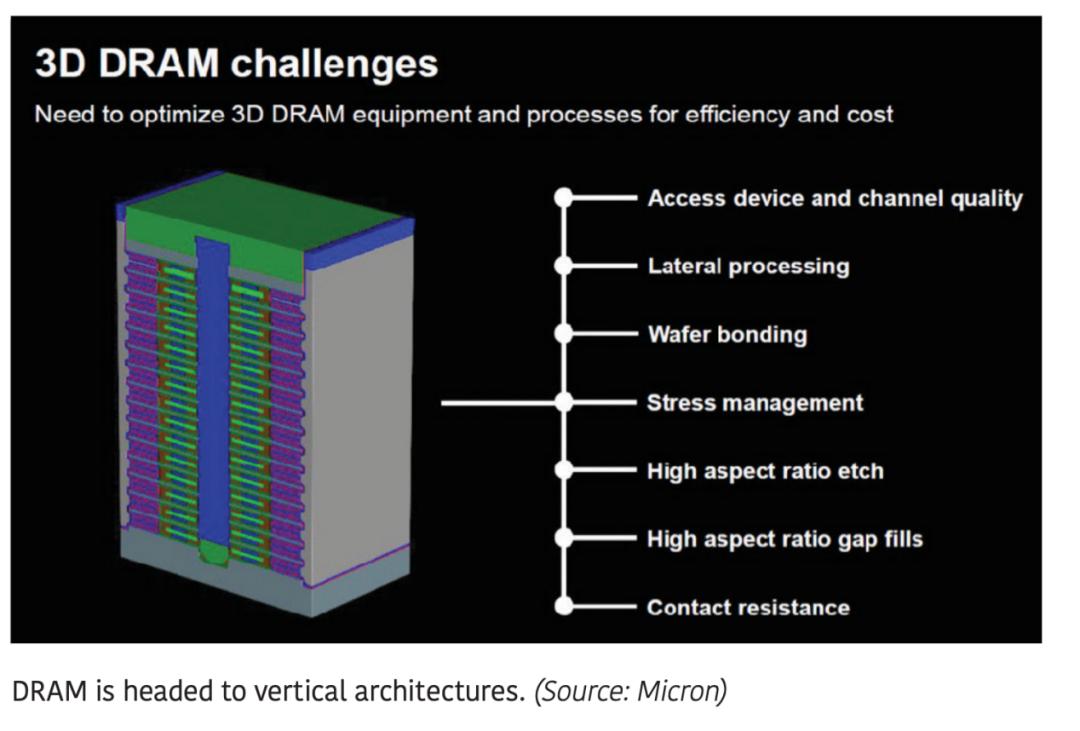
Nirmal Ramaswamy, Vice President of Micron Technology's DRAM Technology Group, said: "Memory products will usher in major changes in the future, including disruptive process and design innovations, next-generation packaging technologies, GPU offloading with advanced inter-chip PHY, and customized (HBM) features."
Ramaswamy pointed out that wafer bonding is the basic technology for DRAM scaling, and emphasized the goal of achieving wafer-to-wafer overlay accuracy below 50nm.
Is Artificial Intelligence Hype or Reality?
At the VLSI Symposium, the question of whether artificial intelligence has formed a bubble, whether it is hype or reality, was raised repeatedly. Ramaswamy from Micron listed a series of industries that will be transformed by AI agents, just like what the programming industry has experienced in the past few years. The industries he listed include healthcare, transportation, manufacturing, finance, agriculture and education. "Every industry we know will usher in changes," he concluded.
As agent-based artificial intelligence becomes popular, agents will call other tools to complete tasks. The infrastructure for edge AI will compete with gigawatt-level data centers for resources.
David Kanter, founder and CEO of benchmarking company MLCommons and an analyst, pointed out that artificial intelligence is starting to make profits. "Anthropic has positive cash flow," he said at the evening panel discussion of the symposium. He also pointed out that as computing demand increases, major cloud service providers are raising prices across the board. "The emergence of artificial intelligence has fundamentally changed software engineering. With the advancement of AI technology, many other fields will also unlock the potential of artificial intelligence," Kanter said.
Moore's Law is Not Dead Yet
If strictly defined as doubling transistor density every few years, Moore's Law may have passed its heyday. But judging from the new foundry technologies demonstrated by manufacturers such as Intel, Samsung, and TSMC at the VLSI Symposium, Moore's Law is still continuously improving in terms of power consumption, performance, and area (PPA) indicators.
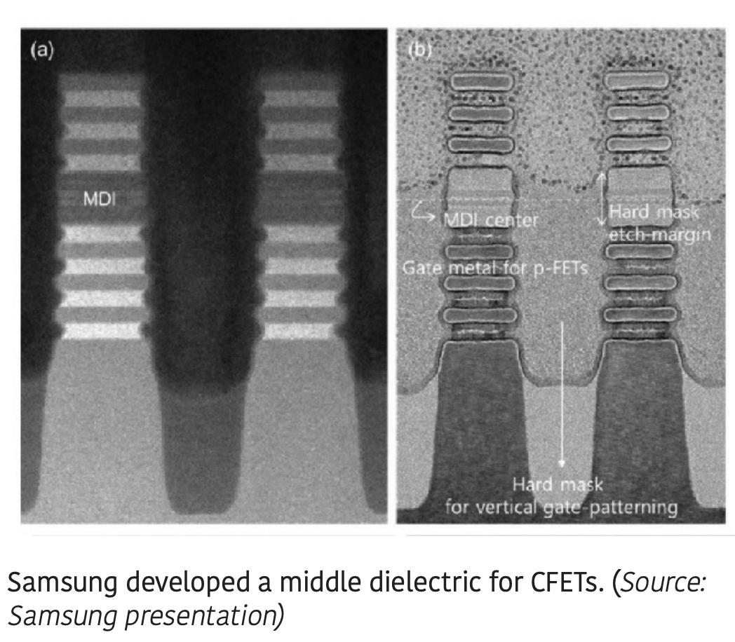
Donghoon Hwang from Samsung presented a future-oriented CFET architecture with multi-nanoribbon channels for N-type and P-type transistors. Its key advances include the use of Middle Dielectric Isolation (MDI) between the top and bottom transistors, as well as the adoption of Through Contact, Top Via, and Common Source-Drain (cSD) designs.
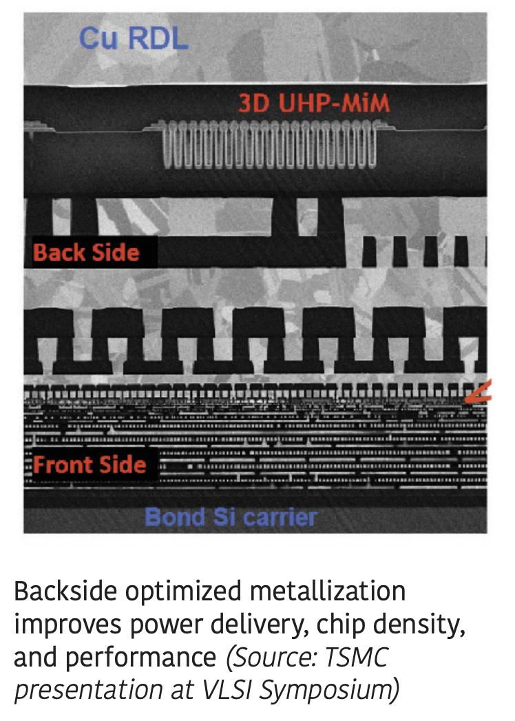
Anupama Bowander from Intel Foundry introduced several improvements to Intel Foundry's 18A-P product, including direct backside contacts, an upgraded backside power delivery architecture, etc. Compared with the 18A product, 18A-P reduces power consumption by 18%, improves heat dissipation performance, and optimizes the bonding layer.
The Power Boost technology of 18A-P adopts a dual-contact architecture, including front-side and back-side contacts. She said that the bottom metal layer uses Extreme Ultraviolet (EUV) lithography technology, which reduces mask costs by 42%. Intel's Nova Lake series processors will be the first to adopt 18A-P technology.
In a subsequent paper, Geoff Yeap from TSMC introduced the foundry's A16 process, which will go into mass production later this year. Compared with the currently fully mass-produced N2 process (which Yeap presented at the 2024 IEDM conference), A16 adopts a "Super Power Rail" backside power delivery scheme with direct contacts, without increasing the area.
Yeap said that compared with N2, the improvements of A16 include: 10% higher transistor density, lower IR drop, 8% to 10% higher speed, and 2% higher SRAM cell density.
"A16 chips are expected to go into production by the end of the year," Yeap said.
Chris Auth, Vice President of Intel, emphasized the importance of paying attention to thermal effects.
"Our EDA tools need to be thermally aware," Auth said. As the industry adopts hybrid bonding technology, packaging becomes more and more important, and the demand for thermal conductive materials is also growing.
"I am a transistor expert, but I think we have only scratched the surface in the field of hybrid bonding," he said.
*Disclaimer: This article is originally written by the author. The content of the article represents the personal view of the author, and Semiconductor Industry Watch reprints it only to convey a different point of view, which does not mean that Semiconductor Industry Watch agrees with or supports this point of view. If you have any objections, please contact Semiconductor Industry Watch.
This article is from the WeChat official account "Semiconductor Industry Watch" (ID: icbank), author: DAVE LAMMERS, authorized by 36Kr for release.