In the past two days, have you tau-ed? Throw away the clumsy and inefficient manufacturing process and embrace system synergy.
Strength can overcome skill, but skill can break through great strength
On May 25, 2026, He Tingbo of Huawei presented the “Tao (τ) Law” at IEEE ISCAS 2026. It replaces “geometric scaling” with “time scaling” and improves transistor density through innovations in devices, circuits, chips, and systems. The company aims to achieve a chip performance equivalent to 1.4nm without EUV by 2031.
On that day, the market value of domestic chip listed companies soared, but the next day, they were hit hard. Except for the packaging and testing sector, almost all sectors declined. More than 4,082 companies saw their stock prices fall, with 34 hitting the daily limit down. The semiconductor and SMIC concept sectors led the decline.
Given the market situation, some people asked which “Tao” the τ refers to. Many people chose “Trap”.

Actually, the Tao Law may sound mysterious, but what it expresses is not complicated. Simply put, the Tao Law answers a question: When it's becoming increasingly difficult to shrink chips infinitely, how can we still improve computing performance? It has nothing to do with the trend of the A-share market.
The losses in holdings may really be due to blind following, and the investors may not really understand what Huawei's Tao means.
01
The Answer of τ in the Post-Moore Era
The reason why the Tao Law has attracted market attention is mainly that in the Moore era, chip manufacturers highly relied on lithography machines. Since ASML stopped supplying due to various reasons, Huawei has been trying to bypass ASML's restrictions. Instead of stuffing more transistors into a unit area, it focuses on making data transfer faster to achieve the efficiency of advanced processes under the original technological path. Coincidentally, the Tao Law can make data transfer faster.
Let's review. The so-called Moore's Law states that the number of transistors on a chip doubles approximately every two years. Generally, the more transistors a chip has, the more powerful it is. So the industry has been struggling to make transistors smaller. From dozens of nanometers to 7nm, 5nm, and 3nm, it's essentially all about “shrinking the size”.
This method was very effective in the past. Just like in a parking lot of the same area, if you make the cars smaller, you can park more cars, and the efficiency will be higher.
However, the problem is that chips are approaching the physical limit. When the size is too small, problems such as severe leakage, overheating, and reduced stability will occur, and the manufacturing cost is becoming increasingly outrageous. An advanced lithography machine is extremely expensive, and the R & D investment is astronomical. That is to say, it's becoming more and more difficult to improve performance by “making it smaller”.
As Moore's Law gradually becomes ineffective, Huawei's Tao Law emerges. “τ (tau)” is a symbol representing the time constant in electronics, which can be simply understood as “the time taken for signal transmission”. The core idea that Huawei wants to express is that in the future, the improvement of chip performance doesn't necessarily have to rely on further shrinking transistors, but can be achieved through “shortening time”.
The Tao Law has a four - level collaborative optimization system, namely the device layer, circuit layer, chip layer, and system layer, which systematically reduces the time constant and drives continuous improvement in performance, energy efficiency, and transistor density.
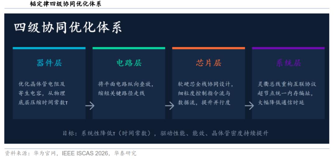
Simply put, in the past, people focused on “how small things are”, but now they focus more on “how fast the data can flow”. In fact, modern chips have a big problem: a lot of time is not wasted on calculation, but on “waiting for data”.
For example, although CPUs and GPUs are very powerful, data needs to be transferred back and forth between memory, cache, and buses, and a lot of time is wasted on the way. This problem becomes more obvious in the AI era. When training large models, the graphics card is not always computing at full capacity; it often waits for data transmission.
So now the entire industry is trying to reduce this “time on the way”. For example, making the chip structure more three - dimensional; shortening the data transmission distance; placing originally scattered modules closer; using technologies such as 3D packaging, Chiplet, and HBM high - bandwidth memory to reduce latency.
These technologies seem to have different directions, but in essence, they are all about the same thing: reducing time consumption.
02
Shorten the Response Time to Seize the Initiative in the Post-Moore Era
The “Logic Folding” proposed by Huawei is actually about compressing the response time to the limit. Many traditional chips have a two - dimensional planar structure, and data needs to travel a long way; while the new design idea is to make the structure more compact and three - dimensional, so that information doesn't have to “travel long distances”, thereby improving overall efficiency.
You can think of it as a city transportation system. The past Moore's Law is like continuously making cars smaller so that the roads can accommodate more cars; while the Tao Law is more like optimizing the entire city transportation: building overpasses, reducing traffic lights, optimizing routes, and shortening commuting distances. Even if the size of the cars remains the same, the overall operating efficiency can still be greatly improved.
Therefore, Huawei's Tao Law does not deny Moore's Law. Instead, it says that in the future, the focus of performance improvement may shift from “spatial scaling” to “time scaling”. In the past, the competition was about “who can make things smaller”; in the future, it may be about “who can make data flow more efficiently”.
Of course, at present, it can't really be called the “new Moore's Law”. The greatness of Moore's Law lies in its effectiveness for several decades, while the Tao Law is more like a new direction and engineering philosophy for the “post - Moore era” and needs long - term verification.
But so far, the Tao Law at least reflects an increasingly obvious trend: in the future, chip competition may not just be about lithography machines and processes, but more about system architecture, data transmission, and overall collaborative efficiency.
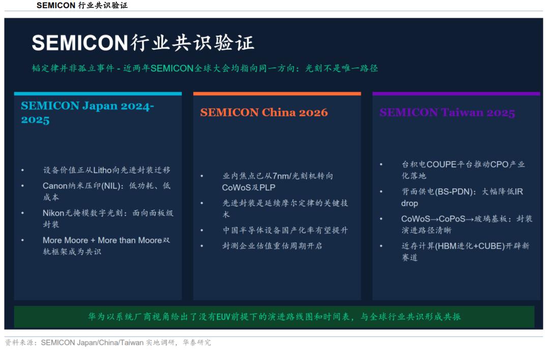
Actually, the current international mainstream technological routes, such as GAA transistors, back - side power delivery, advanced packaging, Chiplet, and CPO optical interconnection, are essentially doing the same thing: reducing energy consumption, shortening latency, and improving system collaborative efficiency. That is to say, the industry has begun to gradually shift from simply relying on “physical scaling” to “system - level optimization”.
From the perspective of the industrial chain, this change may also bring new opportunities. If future performance improvement increasingly depends on 3D stacking, advanced packaging, and system collaboration, then not only the most advanced process manufacturers will benefit, but also the entire industrial chain including packaging, equipment, EDA software, and optical interconnection.
For example, domestic wafer foundries like SMIC and Huahong Semiconductor may gain greater value by combining mature processes with system - level optimization; advanced packaging enterprises, semiconductor equipment manufacturers, and companies engaged in 3DIC design tools and optical interconnection technologies may also become new key directions.
In the long run, what's really important about the Tao Law may not be a specific technology, but it tells the entire chip industry that future chip competition is gradually shifting from “single - point breakthrough” to “full - system collaboration”.
03
How about the Strength of Tao - related Enterprises?
The most intuitive manifestation of full - system collaboration is the continuously demanded computing power in the world today.
As mentioned above, in today's large - model training, GPUs spend a lot of time not computing at full capacity, but waiting for data to be transferred back and forth between HBM, cache, and switch chips. So, the focus of industry competition has begun to gradually shift from “single - chip performance” to “system - level collaborative efficiency”. Those who can make data flow faster, reduce latency, and improve system collaborative efficiency may gain a competitive edge in the next stage.
This is also the really important aspect of Huawei's “Tao (τ) Law”. It points out a new direction in the post - Moore era, bypasses the competition around transistor density in process technology, and relies more on technological routes such as 3D stacking, advanced packaging, Chiplet, optical interconnection, and system collaboration.
This change means a profound restructuring of the global semiconductor industrial chain. In the past, the most core and profitable links were often concentrated in the foundry layer of the most advanced processes; in the future, the importance of advanced packaging, EDA software, optical interconnection, and system architecture design will all rise rapidly.
As repeatedly emphasized in this article, future chips are no longer just about designing an isolated chip. Therefore, at the beginning of the design, it is necessary to design “how the entire system works collaboratively”. This means that not only the most advanced process manufacturers will benefit, but the entire industrial chain. This trend is particularly crucial for the Chinese semiconductor industry.
Because the biggest practical limitation of domestic chips at present is still the inability to freely obtain EUV lithography machines. Under the dominance of Moore's Law, not having access to EUV lithography machines means that there is always a generation gap between China and the world's most advanced processes; but if the industry begins to shift from “competing in processes” to “competing in system collaboration”, Chinese enterprises may have the opportunity to “catch up by changing lanes”.
For example, many people used to think that SMIC was “several generations behind TSMC in terms of processes”. This statement is correct in the dimension of advanced processes, but if we only measure SMIC by “process generation gap”, we will ignore its real industrial value. SMIC is now one of the few global wafer foundries capable of stably mass - producing 7nm - level processes and is also the most complete and mature foundry system in mainland China.
More importantly, in the future “system - level collaboration” route, the importance of mature processes may be re - evaluated. Because many AI chips, edge computing chips, and Chiplet modules do not necessarily all require the most advanced processes. Many functional modules value power consumption, cost, and collaborative efficiency more than the ultimate transistor density.
This means that “mature processes + advanced packaging + system optimization” may completely form a new competitive combination in the future. To some extent, this is also the change happening in the global industry. Even NVIDIA now increasingly relies on CoWoS advanced packaging, not just on the GPU process itself; the competitiveness of Apple's M - series chips also comes not only from the advanced process but also from the software - hardware system - level collaboration.
Therefore, the real strategic value of SMIC in the future may not just be “catching up with 2nm”, but it may become the core foundation of China's post - Moore era system - level manufacturing system. Similarly, although Huahong Semiconductor lags behind SMIC in advanced logic processes, it has strong accumulations in special processes, power semiconductors, embedded storage, etc., and these will also be deeply integrated into the AI, automotive electronics, and edge computing systems in the future.
In addition to the manufacturing end, the changes in the EDA industry are also very worthy of attention. EDA is known as the “mother of chips”. Without EDA software, chip design cannot be completed. In the past, the global EDA market was long - term monopolized by three major American giants, Synopsys, Cadence Design Systems, and Siemens EDA, and they had almost absolute advantages, especially in the fields of advanced processes and complex chip design.
The biggest shortcoming of Chinese EDA in the past was the incomplete tool chain, and many high - end chip designs relied heavily on foreign software. But in recent years, an obvious change has occurred: domestic EDA is gradually evolving from “single - point tools” to a “full - process system”.
For example, enterprises such as Empyrean Technology, Galenics, and Synopsys have begun to make breakthroughs in directions such as analog circuits, IP design, 3DIC, and advanced packaging. More importantly, if the industry focus shifts from “extreme processes” to “system collaboration” in the future, the importance of EDA will further increase.
In the AI era, future chip design will become more and more complex. It's not just about designing the transistors themselves, but about the collaborative relationship between the entire system, including Chiplet interconnection, thermal management, packaging collaboration, optoelectronic co - packaging, etc. All these require the support of a new generation of EDA tools.
In this context, domestic EDA is facing an important window period. Because in the field of traditional advanced process EDA, American enterprises have a very deep advantage, but in the field of next - generation system - level collaborative design, the global industry itself is still in the exploration stage, and Chinese enterprises have the opportunity to narrow the gap in the new track.
Looking back at the entire Chinese chip industrial chain, it not only has the world's most complete electronic manufacturing industrial chain but also the world's largest AI application market. Pushing back from the application layer, this will in turn promote the linkage between EDA, packaging, equipment, manufacturing, and system architecture.
Conclusion
After discussing the technology and industrial logic, it's not difficult to understand why market funds are starting to re - price the semiconductor industrial chain.
In the past, when funds speculated on domestic substitution, the core logic almost revolved around EUV and lithography machines. Because in the traditional Moore's Law era, “advanced process = highest performance = industrial high - ground”. Whoever mastered EUV mastered the chip hegemony; but after the arrival of the AI era, the industry bottleneck has begun to shift from “transistors not being small enough” to “data flowing not fast enough”. The performance competition is shifting from single - chip to system - level collaboration, which means that the importance of 3D stacking, Chiplet, HBM, advanced packaging, CPO optical interconnection, and EDA system - level design is rising rapidly.
For this reason, the market has begun to re - evaluate which are the core assets that will really benefit from the “post - Moore era”: SMIC has continuously hit new historical highs. In essence, it's no longer just about “expectations for advanced processes”, but funds are betting on its strategic value as the manufacturing foundation in China's post - Moore era; Changjiang Electronics Technology has been continuously strengthening, which means that advanced packaging is upgrading from an “auxiliary link” to the core of AI chip performance. In the future, HBM, Chiplet, 3DIC, and high - bandwidth interconnection all highly depend on packaging capabilities.
On the contrary, some traditional “lithography machine concepts” are starting to fall behind. This doesn't mean that EUV is unimportant, but the market has begun to realize that future industry competition is no longer just about “who can reach 2nm first”, but about who can truly integrate manufacturing, packaging, EDA, optical interconnection, AI framework, and data center into a super system.
In a sense, capital has begun to shift from “process thinking” to “system thinking”. In the past, the semiconductor industry competed in transistor density; in the future, it may compete in the collaborative efficiency of the entire industrial chain, and this is exactly where the “Tao Law” really changes the market's perception.