Samsung is experiencing the longest strike in history, but it has lifted the veil on the wealth gap in the AI era.
1 The Samsung strike that sparked global discussions ended before it even started
No one expected that what the global AI computing power frenzy would trigger first was not a chip shortage, but an unprecedented large-scale strike.
Recently, South Korean media have intensively reported the news that Samsung employees are planning a collective strike. The fuse was the breakdown of the latest round of salary negotiations between Samsung Electronics' management and the labor union.
If the two sides still fail to reach an agreement within the final mediation period, starting from May 21st, more than 40,000 employees will launch a large-scale strike lasting 18 days. Samsung's core semiconductor manufacturing department is expected to be directly impacted.

Then a highly dramatic scene occurred.
This ultra-long strike that shocked the global semiconductor circle was put on hold one hour before it was supposed to start.
According to Yonhap News Agency, on May 21st local time, with only one hour left before the scheduled general strike of the Samsung Electronics labor union, the labor and management suddenly reached a preliminary agreement.
The content of the agreement includes that on the basis of maintaining the existing year - end bonus system, the Device Solutions (DS) department of Samsung Electronics, which is responsible for semiconductors, will receive a new special performance bonus. This bonus will only take effect when the operating profit exceeds a certain condition, and the company will take 10.5% of the "performance" as the source of funds. The special performance bonus will be issued in the form of stocks, with no upper limit, for a period of 10 years.
The specific distribution method is as follows: 40% of the funds will be distributed uniformly across the entire DS department, and 60% will be distributed according to the performance of each sub - business unit. According to Yonhap News Agency citing industry forecasts, according to this plan, employees in the memory chip department of the DS department are expected to receive an average performance bonus of 600 million won (approximately 2.72 million RMB) this year.
In addition, in terms of salary, Samsung agreed to raise the average salary by 6.2% this year and improve employees' child - rearing subsidies and housing loan benefits.
However, this is only a temporary preliminary agreement, and whether it can be implemented depends on the final voting result.
Just as Samsung's management used a temporary salary agreement to quell the large - scale strike crisis in the memory chip department, new internal contradictions soon emerged.
Early this morning, according to multiple South Korean media reports, employees in other business departments of Samsung expressed strong dissatisfaction with the above - mentioned agreement. Their dispute is about how to distribute the 10.5% bonus of the operating profit.
According to the agreement, 40% of the funds will be preferentially allocated to the memory department; the remaining 60% will cover all other Samsung business, including wafer foundry, smartphones, TVs, and home appliances. And the bonus itself is directly linked to the future profitability of the HBM (High - Bandwidth Memory) business.
Employees in the DX (Device Experience) department, which is responsible for mobile phones, TVs, and home appliances, believe that the bonus fund pool essentially comes from the AI memory business, rather than the profits created by departments such as mobile phones and home appliances. They question that the current distribution mechanism is further tilting the group's internal resources towards the semiconductor business.
South Korean media revealed that some employees in the memory business may receive stock rewards worth hundreds of millions of won in the future, while the value of the company's shares currently held by employees in the DX department is about 6 million won, with a gap of nearly 100 times between the two.
2 A retrospective of the strike incident
In the past month, about 50,000 Samsung employees planned to go on a 18 - day strike. The fuse was not the company's losses. On the contrary, it was because Samsung was "too rich" but "unwilling to share the money". Facing the record - high profits, employees believed that the company's incentive mechanism did not match their hard work. This situation of "being rich but not sharing" completely ignited the anger of the labor union.
Driven by AI, the demand for HBM soared, and Samsung's semiconductor profits reached a record high. At the beginning of this month, it became the second Asian company after TSMC to achieve such high profits, with a market value of over 1 trillion US dollars.
Early this morning, the market values of Hygon and SK Hynix also exceeded 1 trillion US dollars one after another.
Samsung employees believe that they have not shared in this prosperity in the current booming memory market.
So they put forward several requirements:
• Increase the overall salary raise;
• Cancel the cap mechanism for performance bonuses;
• Link the bonus directly to the company's operating profit;
• Improve the transparency of bonus calculation;
• Establish a long - term, institutionalized profit - sharing mechanism instead of one - time subsidies.
The most controversial one is the OPI/EVA performance system that Samsung has used for a long time.
Samsung's past bonus system was very complex. In essence, it calculated bonuses through indicators such as EVA (Economic Value Added). Employees generally believe that this system is "opaque and has too much room for manipulation". Even if the company's profits soar, the bonuses finally received by employees may not increase synchronously.

The company is making a fortune, but the money distributed to individuals has not increased much. Naturally, Samsung employees are not willing. In addition, some employee incentive measures of SK Hynix, a competitor, have also added fuel to this planned strike. As another chip memory giant, SK Hynix spares no expense in issuing bonuses to employees.
Recently, the news that "SK Hynix employees receive an average bonus of millions of RMB" has spread like wildfire on South Korean social media. There was even an exaggerated statement that "even security guards and drivers can get a bonus of 6 million RMB".
These reports may be exaggerated, but the rewards that Hynix gives to employees are real money.
SK Hynix reached a new agreement with the labor union last year: the company will take 10% of the operating profit as the employee performance bonus pool. That is to say, the more the company earns, the more employees will get. To some extent, it forms a "binding dividend" mechanism.
The calculation of "millions of RMB per person" later was because some South Korean securities firms began to make deductions based on future performance.
For example, many institutions predict that as the demand for AI servers continues to explode, SK Hynix's operating profit in the next two years may further reach a record high. If calculated according to the rule of "10% dividend of profits", in a relatively optimistic situation, the cumulative bonuses of some employees in the next few years may indeed reach an astonishing scale.
However, it should be noted that this is based on the premise that the AI market continues to soar and HBM is in short supply for a long time. It is a forward - looking calculation in the capital market, not the cash that has already arrived.
Even so, the bonuses that SK Hynix has actually issued this year are still enough to make Samsung employees envious.
According to South Korean media reports, SK Hynix issued a large - scale performance bonus to employees at the beginning of this year, with a total amount of up to 4.72 trillion won (approximately 21.2 billion RMB), covering about 35,000 full - time employees. On average, each employee's bonus has reached 140 million won (approximately 650,000 RMB). And the bonus is not just a symbolic distribution, but is truly deeply linked to department profits, individual performance, and job levels. Employees in core positions such as R & D and HBM production get more.
All this happened just when Samsung employees were becoming more and more dissatisfied with the internal salary system.
So before this strike, a key requirement put forward by the Samsung labor union was to allocate 15% of the company's annual operating profit to the employee bonus pool and cancel the original 50% bonus cap.
This is actually quite radical. Because according to the scale of Samsung's semiconductor business, if the AI market continues to be booming, it means that employees' bonuses may reach an extremely exaggerated scale in the future.
But in the end, Samsung did not fully accept the union's plan, but made a compromise. After the South Korean government intervened to mediate, Samsung and the labor union reached the temporary agreement mentioned above at the last moment before the strike, avoiding the originally planned 18 - day large - scale strike.
Mike, an investor who has long been concerned about the semiconductor field, told InfoQ that after this short farce at Samsung ended, it revealed a more dangerous reality: the entire AI industry is being "held hostage" by a very small number of HBM manufacturers. Once there is a problem with the production capacity of any of these manufacturers, the global memory chain will be tightened and may even fall into a supply - cut crisis.
3 Why is HBM important?
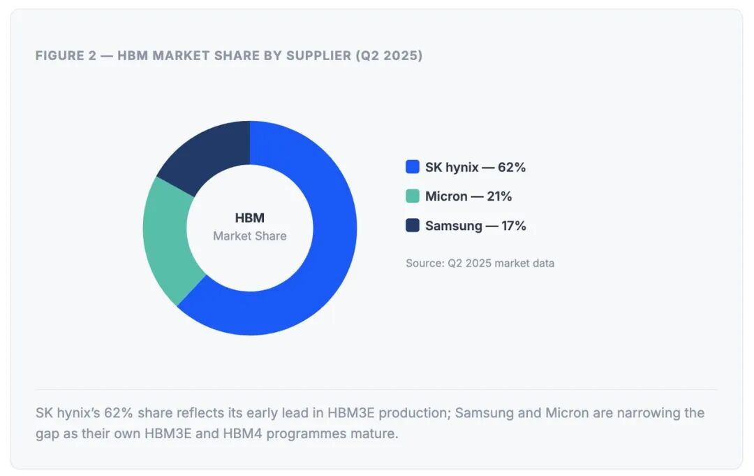
Currently, the global HBM market is highly monopolized by three oligarchs: SK Hynix, Samsung, and Micron. As of the second quarter of 2025, SK Hynix occupies 62% of the market share, thanks to its early exclusive supply agreement with NVIDIA, supplying HBM3E for its H100 and H200 series chips.
Samsung Electronics has a 17% market share and completed the verification of HBM3E in 2025 and started mass production. Micron Technology has a 21% market share and has started shipping 12 - layer HBM3E chips in two configurations: 8 - layer and 12 - layer.
Data source: PatSnap, a SaaS service provider for scientific and technological innovation intelligence
Mike said, "This extreme concentration of supply means that any small fluctuation - whether it is a labor dispute, geopolitical sanctions, or difficulties in improving the technology yield - will be transmitted downstream like a domino effect."
In addition, the market demand for HBM is growing rapidly. The data clearly outlines a "memory hunger" triggered by large - scale AI models.
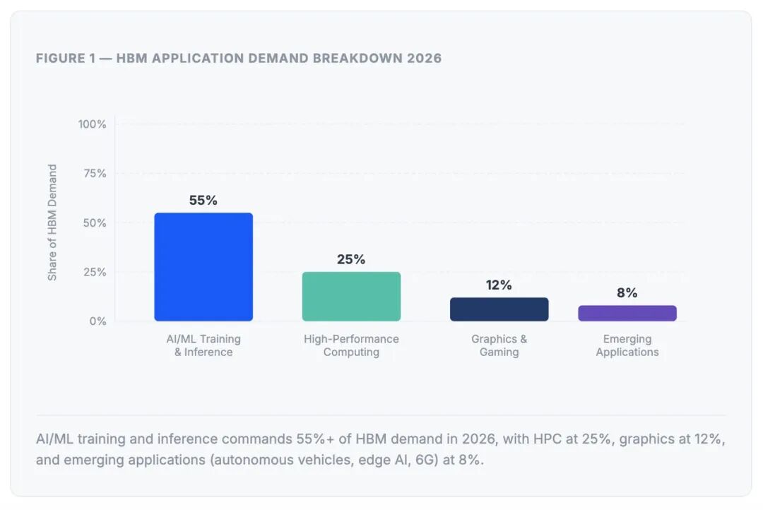
According to PatSnap data, by 2026, AI/ML training and inference will consume more than 55% of the global HBM production capacity, becoming the absolute dominant force.
This crazy consumption stems from a fundamental change in the computing power architecture: whether it is NVIDIA's H200 or AMD's MI350, the engines that support the modern AI edifice, the data throughput width of a single chip has reached 4.8 to 8 TB/s. Only HBM technology can fill this huge bandwidth gap in mass production.
In addition to AI, the core driving force, high - performance computing (HPC) accounts for a quarter of the market share, graphics and games contribute about 12%, and emerging forces such as autonomous driving, edge intelligence, and future 6G infrastructure are dividing the remaining 8%.
This explosive dependence is directly reflected in the capital valuation. In 2024, the HBM market was still in its infancy at 29.3 billion US dollars, but it is expected to soar at a compound annual growth rate of 21.35%. By 2033, the market size will approach 170 billion US dollars.
Mike said, "This indicates that whoever controls the supply of HBM will hold the key to the next - generation digital economy. In the first half of the AI competition, NVIDIA and others may have reaped the benefits, but in the second half, it will be the world of memory manufacturers."
So, why is HBM so important in the AI era?
Lin Feng, a chip design engineer at a domestic intelligent chip factory, told InfoQ, "Whether it is NVIDIA's GPU or the self - developed accelerators of AMD, Google, or Amazon, when competing in performance, it is no longer possible to simply rely on stacking computing cores. It depends on whether and how much data can be 'fed' in."
The GPU is like a super - engine, but if the memory bandwidth cannot keep up, the GPU will idle a lot. Especially in the training of trillion - parameter models, the GPU needs to continuously read parameters, activation values, and intermediate caches at a very high speed. Traditional DDR memory is too far away, has too low bandwidth, and consumes too much power, which can no longer meet the requirements.
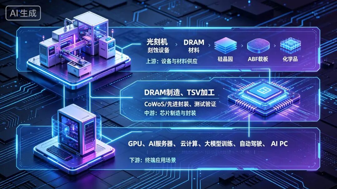
The core value of HBM lies in that through 3D stacking, it vertically stacks multiple layers of DRAM chips like a "skyscraper" and then realizes ultra - wide bus connection through TSV (Through - Silicon Via) technology. Therefore, it is also one of the most difficult processes in the semiconductor industry.
It is really not an easy task to figure out "how to stably stack billions of transistors and a dozen layers of DRAM with a very high yield rate".
It simultaneously tests the capabilities in DRAM process technology, TSV through - silicon via technology, wafer thinning, micro - bump interconnection, thermal management, signal integrity, advanced packaging, and yield control.
Especially as it moves towards HBM3E and HBM4, the number of stacked layers is increasing, and the problems of power consumption and heat generation will increase exponentially.
Currently, HBM technology has developed to the HBM4 stage. According to Lin Feng, according to the latest JEDEC standard, the interface width of HBM4 has been further increased from the previous generation to 2048 bits, with a target bandwidth of 1.5TB/s to 2TB/s, which is twice that of HBM3E. And the currently mass - produced HBM3E is already very impressive.
The bandwidth of a single stack of the current mainstream HBM3E is approximately between 896GB/s and 1.28TB/s. With a 16 - layer stack configuration, the maximum capacity can reach 48GB, which has become the mainstream configuration for AI accelerators in 2026.
The next - generation HBM4 will continue to increase the capacity and bandwidth, with a target single - stack capacity of 64GB. However, the problem is that when the bandwidth doubles continuously, the data transmission, heat control, and signal stability within the system will enter a new difficulty range.
Therefore, the evolution of HBM actually depends on a continuous breakthrough in a whole set of underlying engineering technologies.
Lin Feng believes that the evolution of HBM technology is basically based on four core technology pillars.
The first is TSV, that is, Through - Silicon Via technology. In essence, it drills a large number of micro - through - holes with a diameter of only 10 to 20 microns inside the chip. Through these vertical channels, multiple layers of DRAM are truly "three - dimensionally connected". This is the basis for HBM