The Forced "Tau (τ) Law": A Hidden Experiment Behind Huawei's 381 Chips
On an ordinary weekday in 1965, Gordon Moore, then the director of research and development at Fairchild Semiconductor, sat in his office, writing a special contribution for an industry magazine.
He needed to predict the development of integrated circuits in the next decade, so he casually drew a curve. This curve was very simple: the number of transistors on an integrated circuit would double every 18 to 24 months.
He wrote this observation into his article, titled "Cramming more components onto integrated circuits". It was only four pages long, with no mathematical formulas or rigorous physical derivations. It was more like the intuitive experience of an engineer.
At that time, Moore probably didn't expect that this casually drawn curve would define the evolution rhythm of a trillion - dollar industry for more than six decades.
From the micron, sub - micron to deep sub - micron eras, and from 90nm, 45nm, 14nm all the way to the angstrom era, the iteration of each generation of process nodes is essentially a continuous miniaturization in the spatial dimension: the narrower the width of the transistor gate, the more transistors can be packed into a unit area, and the stronger the performance of the chip.
Simple, direct, and effective. The four words "Moore's Law" were later engraved in the DNA of Silicon Valley and became the collective belief of everyone in the semiconductor industry.
More than fifty years later, this curve can no longer keep up.
The physical wall stands in the way. When the gate is compressed to the scale of a few nanometers, the quantum tunneling current increases exponentially, the control of the gate over the channel decays sharply, and the problems of leakage and variation are insoluble.
The economic wall is even more cruel. The 28nm node is a well - known sweet spot. After that, each generation of nodes requires EUV lithography and multiple patterning exposures. The number of photomask steps doubles, the equipment investment soars, and the cost reduction rate of a single transistor slows down, or even increases instead of decreasing.
The clock of Moore's Law has been demagnetized in the ticking sound.
On May 25, 2026, the IEEE International Symposium on Circuits and Systems opened in Shanghai. He Tingbo stepped onto the podium. The audience was filled with the most core technical forces in the global semiconductor industry, including IEEE Fellows, regulars at top conferences, and the leaders of major IDMs and Fabless companies. Speeches on such occasions are usually about the release of a new chip, but today, the president of Huawei's semiconductor business unit is going to announce a law.
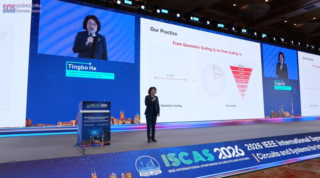
A slide appeared on the screen, showing four characters - "Tao (τ) Law". The scene was silent for two seconds, and then a flurry of shutter sounds rang out.
A slide appeared on the screen, simply showing a few words - "Tao (τ) Law". The scene was first silent for two seconds, and then a flurry of shutter sounds rang out.
This is not an ordinary move. In the more than sixty - year history of the semiconductor industry, there are very few things that can be called "laws".
Moore's Law, Dennard Scaling Law, and Huang's Law have each defined the evolution direction of this industry. Now, the Dennard Scaling Law has been invalid since around 2006, and the entire industry has been wandering at the crossroads of the "post - Moore era" for too long. At this time, a Chinese company steps forward and tries to give its own answer.
"Replace 'geometric miniaturization' with 'time miniaturization'." He Tingbo used this sentence to set the tone for the entire speech.
From the "Miniaturization Race" to the "Time Battlefield"
The core statement of the "Tao (τ) Law" is just one sentence: Replace "geometric miniaturization" with "time (τ) miniaturization" as the new guiding principle for the evolution of semiconductor and electronic systems.

In physics, τ is the symbol for the time constant. In digital circuits, the signal propagation delay is determined by the RC constant, which is the product of resistance R and capacitance C. In other words, what determines the speed of a chip is not only how densely transistors can be packed, but also how fast the signals can travel.
It's easy to understand if you use urban traffic as an analogy.
"Geometric miniaturization" is like continuously narrowing roads and buildings to accommodate more people. As the roads get narrower and the buildings get denser, the marginal benefit decreases.
"Time miniaturization" takes a different approach. Without increasing the city size, it re - plans the road network, builds overpasses, and straightens the key detour routes to make the cars run faster. The transportation volume completed per unit time can still be significantly increased.
In essence, the "Tao Law" extends the performance competition from the density dimension of "how many" to the time dimension of "how fast". When the expansion in space reaches its limit, Huawei chooses to seek answers from time.
The key implementation method is a technology called "Logic Folding".
Traditional chip design has a deep - rooted habit: the metal interconnections between logic units are always restricted to detour on an almost two - dimensional plane. Even though the transistors themselves have long been three - dimensional, the wiring still has to circle in the plane.
If a key path detours too far, the RC delay will become the shortcoming of the entire chip. What "Logic Folding" does is to "fold" the key logic paths on the plane. Through vertical stacking, the wiring length is significantly shortened.
An intuitive analogy: If you pick up goods in a single - layer warehouse, you have to cross hundreds of meters; if you change the warehouse to a multi - layer shelf, moving up and down a few layers is enough, and the movement path is shortened several times.
Logic Folding is essentially a three - dimensional reorganization of the internal logic units of the chip, compressing the physical path of the signal and causing the RC delay to drop sharply. He Tingbo specifically mentioned in her speech that the "Kirin 2026" mobile phone chip is the first complete implementation of this technology. Based on the "free logic" design concept, it has been extended from a single layer to a double layer. This means that Logic Folding has moved from the paper to the silicon chips that can be put into mobile phones.
It's necessary to clarify here that Logic Folding is not the same as the popular 3D packaging in the market.
TSMC's 3DFabric platform, which includes solutions such as SoIC and CoWoS, solves the interconnection between "chips". It vertically stacks Chiplets with different functions such as computing chips and HBM memory, shortening the transmission path between chips.
The interconnection pitch of SoIC has evolved from 6 microns to 4.5 microns, and the signal density of face - to - face stacking can reach 14,000 per square millimeter. These are masterpieces at the physical packaging level.
But the battlefield of Logic Folding is not at the packaging level, but at the design level of the internal logic architecture of the chip.
If 3D packaging is "stacking the built buildings together", Logic Folding is "redesigning the layout of the rooms into duplexes". The former is physical integration, and the latter is design reconstruction.
The two are not in conflict but are complementary. Logic Folding requires the support of a new EDA tool. From the three - dimensional characterization of the standard cell library to the underlying reconstruction of timing analysis, the "folding" at the design level can be completed; and the final physical implementation still requires advanced packaging capabilities to complete the stacking.
Logic Folding is the 3D transformation of "design science", and 3D packaging is the 3D transformation of "physics".
381 Chips and the Equivalent Performance of 1.4nm
The vitality of a law doesn't depend on how beautiful it looks on a PPT, but on whether it has been tested in mass production.
He Tingbo casually mentioned a figure in her speech: In the past six years, Huawei has successfully designed and mass - produced 381 chips based on the Tao Law, covering the entire product line including mobile phone SoCs, AI accelerators, basebands, RF, power management, and automotive applications.
381 chips. This figure means that in the six years when the name "Tao Law" was still completely unknown to the outside world, it had already been regarded as a hidden main line within Huawei, running through the R & D process of a large number of products.
This is not an academic exploration in the laboratory. It is an engineering practice tempered through six years of trials, hundreds of tape - outs, and countless yield improvements.
Logic Folding alone is not enough to systematically reduce the τ of the entire system. Huawei has built a complete multi - level collaborative optimization system, working on four levels simultaneously:
At the device level, start from the atoms.
Optimize the material resistance and parasitic capacitance of transistors and interconnections, which involves the source - drain contact resistance, channel mobility, low - K dielectrics, and the iteration of interconnection metals from aluminum to copper and then to cobalt and ruthenium. A one - percentage - point improvement at the device level may result in a more than ten - percentage - point gain at the system level after being amplified through the circuit, chip, and system levels.
At the circuit level, it is the main battlefield of Logic Folding.
Break through the physical limitations of traditional planar layouts, shorten the wiring length of key paths, reduce the resistance - capacitance load of signal propagation, and directly increase the transistor density and circuit performance. This is the engine of the entire system.
At the chip level, there is full - stack collaboration of "software - architecture - chip".
Perform fine - grained control of instruction streams and data streams according to the actual workload, improve the system - level parallelism, and reduce the end - to - end task completion time. This level is particularly noteworthy: it shows that the Tao Law is not a brute - force task of "squeezing" performance purely by hardware, but a system engineering integrating software and hardware.
At the system level, Huawei has defined a new computing interconnection protocol called "Lingqu Bus", which realizes unified memory addressing and native memory semantics across super - nodes and minimizes the communication delay between multiple chips. From atoms to circuits, from chips to systems, each level serves the goal of reducing τ.
Then there is a more thought - provoking figure. Huawei expects that by 2031, the transistor density of high - end chips based on the Tao Law will reach the equivalent level of the 1.4 - nanometer process.
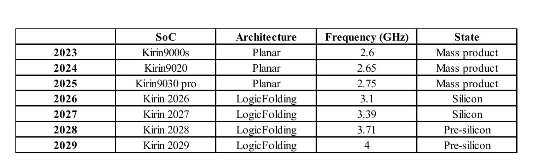
The four words "equivalent level" are worth pondering over and over again.
It means that in the reality where the physical process nodes may still be restricted, through the means of "time miniaturization", an "equivalent approximation" of the most advanced process can be achieved in terms of effective performance and density.
This is actually answering a question that the Chinese semiconductor industry cannot avoid: If the next - generation lithography machine cannot be obtained, and if the miniaturization of physical feature sizes is stuck, can chips equivalent to the most advanced process still be produced?
The answer that Huawei gives now is: Yes. The path has changed.
Epilogue
Looking at the Tao Law in the global semiconductor game in 2026, the tripartite pattern is clear at a glance.
Intel has chosen "device innovation".
It replaces FinFET with RibbonFET full - surround gate and moves the power network from the front of the chip to the back with PowerVia, aiming for performance and energy efficiency in the 18A process. This path is essentially a final sprint on the geometric miniaturization track and a loyal relay of Moore's Law.
TSMC has chosen the "packaging revolution".
The 3DFabric platform densely interconnects Chiplets of different process nodes within the package. The CoWoS with a 5.5 - times photomask size has been mass - produced, and more radical solutions are on the way. According to industry forecasts, the 2.5D/3D advanced packaging market will approach $35 billion by 2030. This is the "integration paradigm" of physical stacking - stacking everything that can be stacked together.
Huawei's Tao Law takes a third path, "design reconstruction".
It does not exclude devices and packaging. Logic Folding itself requires advanced devices and 3D packaging capabilities as a foundation. But its core insight is that starting from the dimension of design paradigm rather than manufacturing process, it re - defines where the engine of chip performance growth lies.
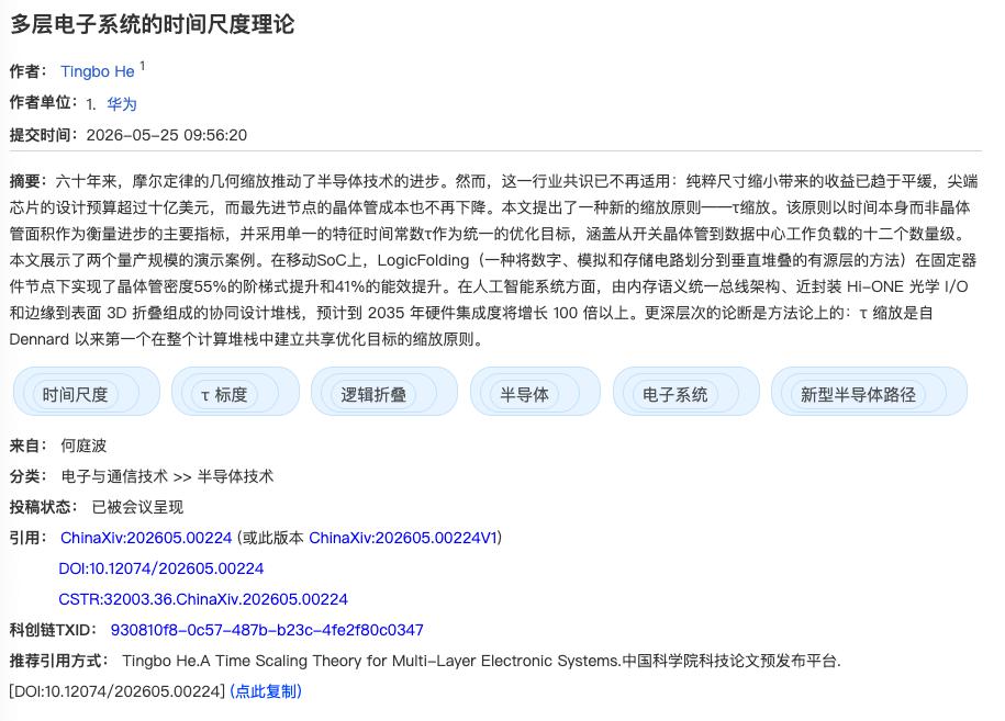
One background cannot be ignored. This law is proposed by a company that has long been restricted by the supply of advanced processes. In a sense, this is an innovation forced out of necessity.
When one path is blocked, you only have one choice to answer the most fundamental question: Besides making transistors smaller, is there any other possibility for the growth of chip performance? 381 chips, six years of silent practice, and unknown R & D investment are all the costs of this answer.
He Tingbo left a sentence at the end of her speech: "The future must belong to open cooperation. On the path of semiconductor evolution, no single company can complete all the answers alone. Under the path of the Tao (τ) Law, we look forward to close cooperation with global scientists, engineers, and industry partners to jointly promote the continuous development of the semiconductor and electronic industries."
From 2026 to 2035, Huawei plans to push Logic Folding from double - layer to full - scale folding, or even more layers of folding. This is a long - distance race measured in at least a decade.
The end of an era is often the prologue of a new paradigm. Sixty - one years ago, the exponential curve casually drawn by Moore in the office of Fairchild Semiconductor once defined what progress was.
In the past sixty years, the entire industry believed that the number of transistors was power. When the physical wall and the economic wall stand in front at the same time, the one - way street finally branches. Intel breaks through head - on, TSMC does physical stacking, and Huawei has marked out an uncultivated territory in the dimension of "time" that was once ignored.
Today, a solution from the East tries to remind the world: When the expansion in space reaches its limit, seeking answers from time may be the only way to the next stage.
Can this answer support the next sixty years? Time, the constant τ written into the law's name by Huawei, will be the final judge.
Disclaimer: This article is written based on publicly available information or information provided by interviewees, but Decode and the author