Hard Kr Exclusive | The academician team from University of Science and Technology Beijing has founded a 2D semiconductor startup, securing tens of millions of RMB in financing from investors including Inno, CAS Star and other institutions.
Author | Qiu Xiaofen
Editor | Yuan Silai
36Kr has learned that two-dimensional semiconductor company Beike Tiangong Tianxin (Beijing) Technology Co., Ltd. (hereinafter referred to as "Tiangong Tianxin") has recently completed tens of millions of yuan in seed round financing, with investment from CAS Star and Inno Fund. The funds raised in this round will be mainly used for team building, wafer production capacity construction and transformation of technological achievements.
Established in May 2026, "Tiangong Tianxin" is a scientific and technological achievement transformation project led by the team of Academician Zhang Yue from University of Science and Technology Beijing, focusing on opening up the full technical chain of two-dimensional semiconductors from material production to chip manufacturing.
Tiangong Tianxin
Among them, Zhang Yue, academician of the Chinese Academy of Sciences, serves as the chief strategic scientist; Zhang Zheng, co-founder and CTO, is a professor at University of Science and Technology Beijing and a recipient of the National Science Fund for Distinguished Young Scholars. In addition, the company has also absorbed industrial talents from leading enterprises in the integrated circuit sector.
Two-dimensional semiconductor is one of the key new material directions under exploration in the global semiconductor industry in recent years.
Over the past few decades, the continuous improvement of chip performance has mainly relied on the miniaturization of transistor size. However, as advanced processes move to 2nm and smaller nodes, traditional silicon-based transistors are facing physical limitations such as short-channel effect and increased leakage current, and the technical difficulty and manufacturing cost of continuing to shrink the size keep rising.
For this reason, two-dimensional semiconductors are regarded as one of the potential solutions to extend Moore's Law. Represented by molybdenum disulfide and tungsten diselenide, silicon channel materials can reach the thickness of a single atomic layer, which is not only expected to improve the leakage problem of transistors at extremely small sizes and reduce chip power consumption, but also has the potential to be compatible with the existing silicon-based manufacturing process, without completely overturning the existing production line and equipment system.
In the past, two-dimensional semiconductors remained in the stage of academic research for a long time. In the past two years, an obvious change is that leading global semiconductor enterprises have begun to accelerate their layout in this field.
For example, enterprises including IMEC and TSMC are continuously promoting the research of two-dimensional semiconductor transistors and wafer-level integration; Samsung is also exploring the production of large-size molybdenum disulfide materials; Intel has also included two-dimensional semiconductors in its future research direction for advanced devices. With the in-depth participation of the industry, the commercialization of two-dimensional semiconductors is progressing faster than the outside world expected. In the next two to three years, the number of transistors will see an order of magnitude growth, and major breakthroughs will also be achieved in functions and performance.
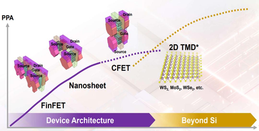
Image authorized by the enterprise
Zhang Zheng, co-founder and CTO of "Tiangong Tianxin", introduced to 36Kr that two-dimensional semiconductor is the most competitive new material for processes below 1nm in the future, and is expected to be firstly applied in fields such as edge computing, computing-in-memory, sensing-computing-in-memory and space computing power.
However, it is not easy for two-dimensional semiconductors to truly enter the mass production of advanced process chips. The first challenge lies in the preparation of large-size, high-quality wafers: to make the atomic-thickness material uniformly cover the entire wafer while ensuring the consistency of crystal quality, defect density and device performance, the difficulty has increased significantly.
Therefore, one of the core technologies of "Tiangong Tianxin" is the team's original two-dimensional melting confinement "Zhang's Growth Method". According to the introduction, this technology uses molten glass to assist growth, realizing the preparation of large-size single-crystal two-dimensional semiconductor materials. Relevant achievements of the team were published in *Nature Materials* in 2025.
According to the company's disclosure, the team has realized the preparation of 2-inch single-layer molybdenum disulfide single crystal wafers, with the material thickness of about 0.65 nanometers, the device yield rate within the centimeter-level range exceeds 96%, and the team has recently completed the development of 8-inch equipment and process development.
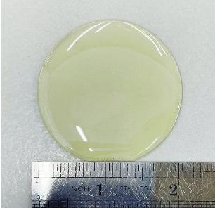
Image authorized by the enterprise
However, material growth is only the first step. For two-dimensional semiconductors to truly enter the chip industry, a series of problems need to be solved, including material transfer, metal contact, etching, dielectric layer integration, and compatibility with existing silicon-based processes.
To this end, the team has long-term accumulation in these links. Specifically, at the transistor level, the team originally proposed the idea and technical method of atomic layer bonding, and for the first time developed a two-dimensional transistor device that meets the thermal budget requirements of the back-end integration process. All performance indicators fully exceed the requirements of the International Roadmap for Devices and Systems (IRDS), which effectively promotes the development of two-dimensional semiconductor devices from laboratory research to engineering manufacturing. This achievement was selected as one of the Top 10 Advances in Chip Science in China 2025.
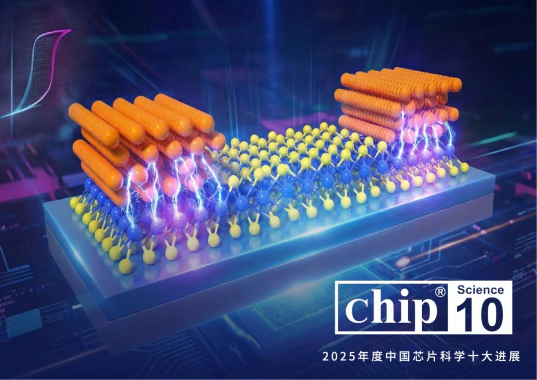
Image authorized by the enterprise
At the circuit architecture level, the company proposed a new Pseudo-CMOS architecture, and developed a low-power logic operation unit through new device and circuit design methods.
According to the research results disclosed by the company, the team has developed a two-dimensional semiconductor logic circuit with power consumption of only about 2% of that of similar silicon devices.
Compared with single-point technological breakthroughs, "Tiangong Tianxin" puts more emphasis on full-process manufacturing capabilities. At present, the team has established a cooperative R&D mechanism relying on the 6-inch two-dimensional semiconductor R&D platform built by University of Science and Technology Beijing and the first domestic 8-inch two-dimensional semiconductor pilot production line.
Among them, the 6-inch platform is mainly responsible for R&D of materials, devices and processes, while the 8-inch pilot line is oriented to wafer manufacturing, process integration and small-scale mass production verification.
According to the introduction, the production capacity of a single 8-inch MOCVD molybdenum disulfide and tungsten diselenide wafer equipment of "Tiangong Tianxin" is about 15 pieces per day. The next step will focus on improving material size, batch stability and production efficiency.
In terms of business model, "Tiangong Tianxin" plans to provide industrial customers with large-size wafers, special production equipment, process development and related technical services in the future. It is understood that the team has carried out technical cooperation and exchanges with industrial enterprises such as Unigroup and Empyrean.
In the longer term, "Tiangong Tianxin" also hopes to explore open foundry services, and finally form an IDM platform covering materials, processes, design tools and chip manufacturing.
Zhang Zheng also holds a relatively prudent judgment on the long-term prospect of two-dimensional semiconductors. He believes that two-dimensional semiconductors are not intended to completely replace silicon-based chips, but to integrate with existing silicon-based processes and achieve breakthroughs in some key material and device links.
The following is the exchange between 36Kr and Zhang Zheng (abridged)
36Kr: What is the current industry trend of two-dimensional semiconductors?
Zhang Zheng: At present, there are two main technical routes in the industry. One is 3D integration, such as Chiplet, HBM, etc., which is equivalent to building higher "buildings" to endow chips with stronger computing power. The other direction is to continue to reduce the size of each transistor, that is, process miniaturization.
However, the future development of integrated circuits is facing the limit of size miniaturization. In the process of continuous size reduction, silicon material has encountered an insurmountable bottleneck, that its thickness can hardly be less than 6 nanometers. At this time, new materials are needed to continue the development trend of existing silicon materials and extend Moore's Law. Two-dimensional semiconductors have naturally become an important layout direction in the future.
TSMC, Samsung, Intel, and Tokyo Electron this year have all proposed in their own technical roadmaps to take two-dimensional semiconductor materials as a key node in future processes.
36Kr: What effects will be brought after replacing silicon channel materials with two-dimensional semiconductors?
Zhang Zheng: The main challenge faced by silicon materials in the process of size miniaturization is that a larger voltage is required to drive the device to obtain better current, which will bring higher power consumption, more leakage current, and higher static power consumption.
One of the biggest advantages of two-dimensional semiconductors is the extremely low static power consumption. Its leakage current level is about 1/1000 of that of silicon, and the resulting static power consumption performance can be more than 10 times lower. For future large computing power chips, this power consumption advantage will be very significant.
The second advantage is that the material itself has a van der Waals heterostructure. Unlike traditional materials that mainly combine with the substrate and other materials through chemical bonds such as covalent bonds and ionic bonds, it forms a structure through van der Waals forces.
The benefit of this interaction mode is easy integration. Its integration with traditional processes does not fully rely on epitaxial growth. It is more like building Lego blocks, which can be assembled layer by layer to realize three-dimensional or vertical integration, making it easier to be compatible with existing processes during the integration process.
36Kr: What are the difficulties in the actual implementation of two-dimensional semiconductors?
Zhang Zheng: Two-dimensional semiconductors adjust the channel material, which is equivalent to making changes from the very beginning of the entire chip manufacturing process, and thousands of subsequent processes need to be adjusted adaptively. The integrated circuit itself is a closed-loop R&D system, including materials, equipment, processes, standards and design. To complete this closed loop, verification needs to be carried out one by one at different process nodes, so the R&D cycle itself will be relatively long. I have always described the industrialization development of this field as moving forward in fluctuations and rising in spirals.
36Kr: What chip fields will be the most valuable application scenarios for two-dimensional semiconductors in the future?
Zhang Zheng: The ultimate goal is definitely advanced process computing power chips, that is, logic chips, which is the final application scenario of two-dimensional semiconductors.
But in recent years, we will also have some phased application opportunities. The biggest advantages of two-dimensional semiconductors are low power consumption and easy integration, so in the short term, there may be large application space in fields such as end-side computing and sensing-computing-in-memory.
Another relatively large application scenario is space computing power chips. Two-dimensional semiconductor materials are only as thick as a single layer of atoms, and radiation particles in the universe can pass directly through the material without staying inside the two-dimensional semiconductor, so it has very strong radiation resistance.
36Kr: What is the relationship between two-dimensional semiconductors and silicon-based materials? Will they replace silicon in the future or form complementarity with silicon?
Zhang Zheng: My teacher, Academician Zhang Yue, the chief scientist of our team, has always emphasized that "two-dimensional semiconductors are not meant to replace silicon. What we are taking is a new track that integrates with silicon-based materials and develops in compatibility with silicon-based processes". In future computing power chips, two-dimensional semiconductors and traditional silicon-based materials both play important roles, which can form a good complement and jointly build the technical base for the artificial intelligence era.
Homepage image source | AI synthesis

end