Everything You Need to Know About Optical Modules (Part 2): Optics Moves Closer to Chips, How Exactly Do AI Data Centers Speed Up?


In 1976, the Cray-1 supercomputer was launched. It bent the rectangular cabinet into a huge C-shape, with soft padding wrapped around the outer ring, looking like a set of circular sofas from a sci-fi movie.
This design serves a clear goal: boost speed. The total length of internal wires inside the Cray-1 exceeded 60 miles, but the C-shaped chassis brought components close to each other, ensuring that no segment of the wire was longer than 3 feet.
This compact layout helped reduce signal latency, and was also one of the key factors for the Cray-1 to take the lead in performance at that time.

Nearly half a century later, AI data centers are facing a similar proposition: let signals travel a shorter distance.
Today, in a large number of high-speed cross-cabinet connections, data between servers needs to be transmitted through optical fibers. But before entering the optical fiber, data still has to leave the switching chip in the form of electrical signals first, travel along the circuit board to the optical module on the device panel, and then be converted into optical signals.
In the past, this distance calculated in centimeters was negligible; now, it has begun to become a bottleneck affecting system efficiency.
As a result, the industry began to reconsider the position of photoelectric conversion: can we shorten the transmission distance of electrical signals on the circuit board, so that data can be converted into light earlier after leaving the switching chip?

The ultimate engineering of optics approaching chips
CPO (Co-packed Optics) is precisely targeting this distance. It places the optical engine responsible for photoelectric conversion next to the switching chip and integrates it into the same packaging system. As soon as the data leaves the switching chip, it turns into light after a very short electrical connection, and then is sent out of the device through the optical fiber.
CPO is often regarded as one of the "ultimate" forms of optical interconnection.
First of all, CPO can shorten the high-loss electrical channel, reduce the power consumption brought by high-speed signal processing, and has the opportunity to reduce transmission latency. Secondly, the optical engine is no longer concentrated in the pluggable modules on the front panel of the device, so the switch can accommodate high-speed ports with higher density.
More importantly, when the AI cluster expands to hundreds of thousands or even more GPUs, network power consumption, port failures and link interruptions may all turn into idling of expensive computing power. What CPO tries to reduce is the system cost paid by the entire network in data transmission, heat dissipation and signal processing.
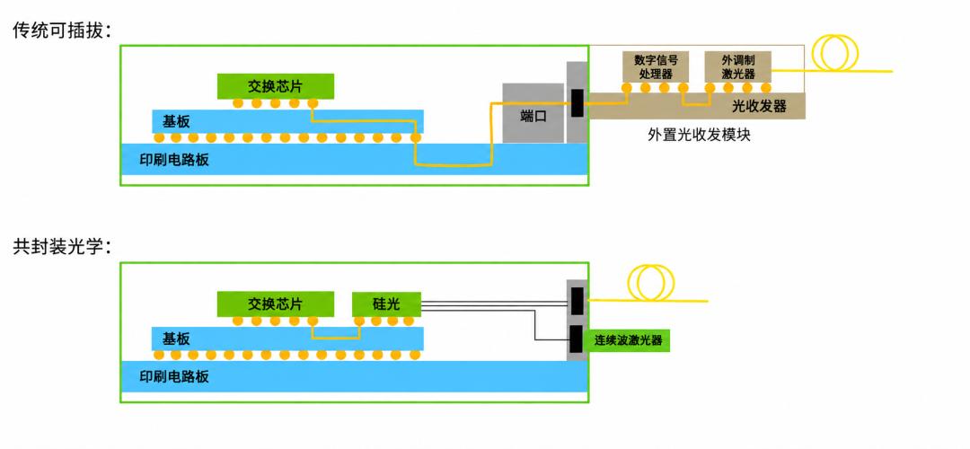
NVIDIA is one of the enterprises actively promoting the implementation of CPO. At the GTC 2025 conference, NVIDIA first released its CPO product, Spectrum-X Ethernet Photonics.
According to the comparative data released in 2026, NVIDIA claims that compared with traditional pluggable modules, this solution can achieve 5 times power efficiency and extend the continuous running time of AI applications to 5 times.
At present, this product has entered the full mass production stage. Cloud service providers and AI infrastructure providers including Oracle, Microsoft, Meta and CoreWeave have become the first batch of customers.
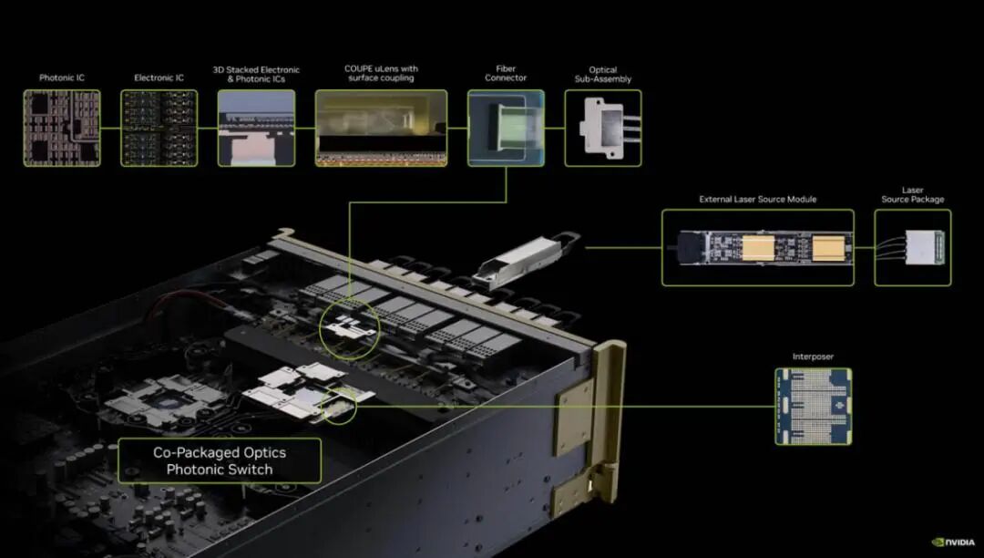
NVIDIA CPO
However, the so-called "ultimate" also implicitly reflects that CPO is not easy to implement. It still needs to cross a threshold: mass production.
The first is precision coupling. Light needs to enter the optical fiber with a core diameter of only a few micrometers from the chip. Once there is a tiny deviation in position, the received optical power may drop significantly. The more optical fibers and ports there are, the higher the requirements for alignment speed, accuracy and consistency.
After entering the co-packaging system, the optical engine is more closely integrated with the expensive switching chip, so testing needs to be moved forward to different stages such as wafers, chips and packaging. The later the test problem is found, the more devices may need to be scrapped.
Thermal management is also unavoidable. The switching chip is a major heat generator in the device, but lasers and some optical devices are very sensitive to temperature. Therefore, some CPO solutions leave the lasers outside the package, and then supply light to the internal optical engine through optical fibers, so as to reduce the impact of high temperature on the service life and stability of the light source.

NVIDIA's ability to take the lead in promoting CPO mass production is related to its simultaneous mastery of GPU, network card, switching chip, network software and whole machine architecture, and it is also inseparable from the early collaboration of industrial chain enterprises such as TSMC, SPIL, TFC, Coherent, Lumentum and Corning.
Overall, the current threshold for CPO is still relatively high. According to the report released by TrendForce in March 2026, CPO will account for about 0.5% of the optical modules used in AI data centers this year.
Therefore, the industry has also turned its attention to a more easily implemented compromise option — NPO.

A more pragmatic compromise solution
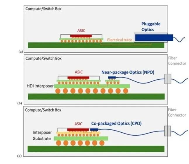
NPO (Near-packaged Optics) also moves the optical engine from the switch panel to the inside of the device, placing it near the switching chip, thereby shortening the transmission path of high-speed electrical signals on the circuit board.
However, the optical engine still retains an independent package and can be installed and disassembled through sockets or other connecting structures.
This allows NPO to retain the value of both aspects: compared with traditional pluggable optical modules, it shortens the transmission distance of electrical signals, has the opportunity to reduce power consumption and improve port density; compared with CPO, the optical engine can be tested independently, and it is easier to repair or replace.
The NPO market is entering a stage of accelerated ecological construction, and large-scale commercial use has also received more attention in 2026. According to market sources, tens of thousands of NPO products ordered by Google have been delivered successively since May 2026, and mass production is expected to be realized in 2027. TrendForce predicts that the combined market size of CPO and NPO will exceed 39 billion US dollars in 2030.
NPO still needs time to achieve full-scale volume shipment, but its practical value has already emerged: it can not only help enterprises accumulate production and operation experience of near-packaged optics, but also meet the data center's requirements for independent testing, replacement and maintenance of optical engines.
Behind NPO and CPO, there is an important technical support — silicon photonics.
Most traditional optical modules adopt the discrete device assembly mode, which requires assembling and aligning devices such as lasers, modulators, detectors and optical splitters one by one.
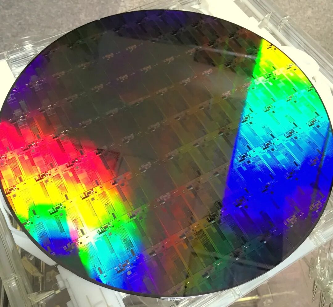
Silicon photonics draws on the manufacturing process of integrated circuits, and integrates devices such as waveguides, modulators and photodetectors on a silicon-based photonic chip. This integration method can reduce the device size, shorten the internal connection, and is more suitable for expanding production through wafer-level processes.
It must be pointed out that the application of silicon photonics is not limited to NPO and CPO, and it can also be used in traditional pluggable modules. Today, some silicon photonic chips can deploy hundreds of devices within a range of square millimeters; the integration scale of some research chips has reached thousands or even tens of thousands.
As a result, the current optical communication industry has two paths advancing at the same time: silicon photonics integrates the originally scattered optical devices onto the chip, while NPO and CPO make the optical engine move closer to the switching chip.
When chip integration and packaging architecture change at the same time, the original division of labor in the global industrial chain will loosen accordingly.

Restructuring of the optical communication industrial chain
The global optical communication industrial chain has long shown a pattern of transnational collaboration, and different regions have their own advantages in links such as materials, chips, devices, packaging and large-scale manufacturing.
The upstream mainly includes optical chips and electrical chips. Optical chips are the core components that complete photoelectric conversion; electrical chips are mainly responsible for driving optical chips, as well as amplifying and processing high-speed electrical signals.
The optical chip industry in Europe, America and Japan started earlier, and relevant enterprises have accumulated core technologies and manufacturing processes with first-mover advantages. At present, domestic enterprises in China have also begun to test and verify domestic optical chips, seek domestic substitution, and promote the optical chip industry to improve the level of independent control.
It is worth mentioning that the manufacture of some optical chips requires a key semiconductor substrate material — indium phosphide. The supply of metal indium required for indium phosphide is highly concentrated, and China's refined indium output accounts for 70% of the total global output.
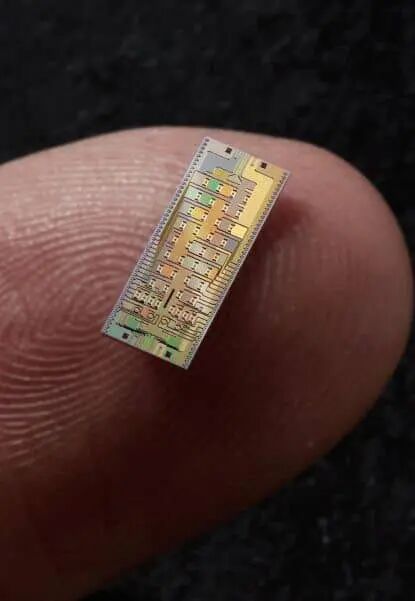
The midstream of the industrial chain mainly includes optical devices (some views classify them as upstream links) and optical modules.
Optical devices are the core components of optical modules, which will directly affect the performance and stability of optical modules. Although the high-end optical device market has long been dominated by manufacturers in the United States, Japan and other countries, Chinese manufacturers have also begun to supply customers around the world. For example, TFC has entered NVIDIA's CPO partner system.

In the optical device packaging link, since it is necessary to integrate upstream chips with other optical devices, this link is closely related to chip design and manufacturing processes. Vertically integrated manufacturers including Coherent and Lumentum, as well as professional enterprises focusing on optical devices, precision packaging or system assembly, are all important participants.
For optical modules, this link involves precision coupling, packaging, testing and large-scale delivery of various optical components, which is one of the links where Chinese enterprises have the most concentrated advantages.
According to the list released