Equipment giants are vying for advanced packaging
In early October, a piece of news in the capital market drew widespread attention: over concerns that ASML may enter the hybrid bonding equipment market and the demand for HBM-related equipment will be postponed, Bank of America downgraded the investment rating of Besi, a Dutch packaging equipment manufacturer, on October 6, driving its share price down 5.39% on the same day; the next day, as UBS further downgraded its rating, Besi's share price fell another 8.49%, with a cumulative drop of about 13.4% in just two trading days. In fact, ASML delivered the TWINSCAN XT:260 lithography system for advanced packaging as early as 2025, and news of its R&D of hybrid bonding equipment came out this year, further expanding its business beyond traditional lithography.
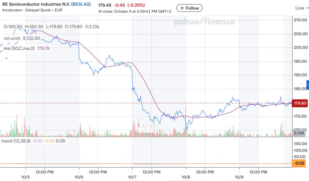
Overview of Besi's stock price trend (Source: Yahoo)
Meanwhile, Applied Materials and Lam Research are also accelerating their layout. In the first week of October alone, Applied Materials successively announced deepened cooperation with Besi and Intel, with R&D scope covering hybrid bonding, TCB, chip-to-panel, Foveros 3D packaging and other technologies. Leveraging technologies such as etching, deposition and copper electroplating, Lam Research continues to expand its equipment layout in the fields of TSV and 3D interconnection. In March this year, Reuters reported that both Lam Research and Applied Materials showed acquisition interest in Besi.
It can be seen that the three giants of front-end equipment are extending to advanced packaging along different technical routes. On the one hand, the front-end equipment giants are actively extending to advanced packaging, and on the other hand, the traditional leading packaging equipment manufacturers have become the targets of cooperation, investment and even potential mergers and acquisitions. The originally relatively clear division of labor between front-end and back-end in the semiconductor equipment industry is undergoing subtle changes. Advanced packaging is becoming a new battlefield that semiconductor equipment giants are vying to enter.
The Three Front-End Equipment Giants Are Surrounding Advanced Packaging
In fact, a closer look shows that although Applied Materials, Lam Research and ASML are all extending to the advanced packaging field, the three have chosen different entry methods.
Applied Materials pays more attention to material engineering and process integration, and builds comprehensive solutions covering multiple manufacturing links by cooperating with professional packaging equipment manufacturers; Lam Research relies on etching, deposition and copper interconnection technologies to compete for more and more key process steps in the 3D integration process; ASML has begun to try to extend its accumulated nanoscale motion control, precision alignment and measurement technologies in the lithography field to hybrid bonding equipment.
These three routes are complementary to each other, and may gradually form direct competition as technology evolves.
Applied Materials: Join hands with Besi to build a complete process chain
First of all, talking about Applied Materials, its layout in advanced packaging has actually lasted for many years.
As early as 2020, Applied Materials and Besi established a joint R&D project in Singapore, combining its own technologies in etching, planarization, thin film deposition, wafer cleaning, metrology and inspection, and particle control with Besi's capabilities in precision chip mounting, interconnection and assembly.
The representative achievement of the cooperation between the two parties is the Kinex integrated Die-to-Wafer (D2W) hybrid bonding system. Different from traditional packaging equipment that mainly focuses on chip mounting and connection, Kinex attempts to integrate pre-bonding processes such as surface treatment, cleaning, activation and alignment into a more compact manufacturing flow.
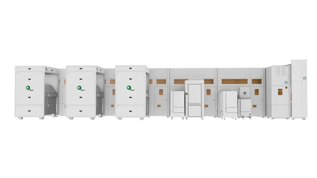
Kinex (Image source: Applied Materials)
This design has practical significance.
In the hybrid bonding process, the two chips or wafers to be connected must not only achieve extremely high-precision geometric alignment, but also ensure the flatness, cleanliness and material state of the bonding surface. Even if the bonding equipment itself has excellent positioning accuracy, if the previous process causes particle pollution, abnormal copper pad depression or unstable surface state, it may still lead to connection defects. The cooperation between Applied Materials and Besi is essentially an attempt to combine traditional front-end material engineering with back-end precision assembly technology to improve the final yield through cross-process collaboration.
It is worth noting that Applied Materials does not limit technical cooperation to Besi alone. Previously, it also cooperated with EV Group (EVG), an Austrian wafer bonding equipment manufacturer, to develop wafer-to-wafer bonding solutions.
The cooperation upgrade on October 1 this year further expanded the R&D boundary of both parties. According to the official announcement, Besi will become an innovation partner of Applied Materials' EPIC R&D center located in Silicon Valley. In the future, the two parties will not only continue to promote D2W hybrid bonding, but also jointly research TCB process scaling, chip-to-chip, chip-to-panel and new integration architectures for optical interconnection. The EPIC center is planned to have a maximum investment scale of about 5 billion US dollars, and the investment will be gradually rolled out as customer projects advance. An important goal of this center is to enable chip manufacturers, equipment suppliers and material enterprises to participate in joint R&D at an earlier stage, shortening the cycle for new processes to move from the laboratory to mass production.
From the perspective of industrial significance, this means that Applied Materials is trying to incorporate advanced packaging, which was previously a relatively independent back-end manufacturing link, into its broader material engineering R&D system.
Just five days later, Applied Materials announced the deepening of cooperation with Intel, covering R&D of next-generation transistors, on-chip interconnection and Foveros 3D advanced packaging.
These two cooperations seem to target different enterprises, but their technical logic is connected. In 3D stacking, there are complex interactions between interconnection density, power supply paths, heat dissipation structures and material stress between chips. The performance optimization of next-generation chips is increasingly difficult to achieve by relying solely on one link among advanced process, metal interconnection or packaging.
Therefore, for Applied Materials, the real strategic value may not only be to obtain more orders for hybrid bonding equipment, but to participate in the definition of next-generation chip manufacturing processes earlier through the joint development of front-end and back-end processes. As Prabu Raja from Applied Materials asserted: Advanced packaging is no longer just the physical assembly of the back-end, but a material engineering revolution that requires wafer-level precision and cleanliness.
Lam Research: From Etching, Deposition to 3D Interconnection
Compared with the cooperation model between Applied Materials and Besi, Lam Research's layout in the advanced packaging field highlights its existing process and equipment advantages. Lam Research has accumulated a large number of high-aspect-ratio etching, thin film deposition and metal interconnection technologies in the past in the manufacture of logic chips, DRAM and 3D NAND.
With the continuous 3D development of advanced packaging, these technologies are gaining more application scenarios. For example, in 3D stacked chips, Through-Silicon Vias (TSVs) undertake vertical electrical connections between different chip layers. To make deep and narrow vias in silicon wafers, high-aspect-ratio etching technology is required, and the via sidewall morphology, etching uniformity and defect control should be guaranteed as much as possible.
Lam Research's Syndion deep reactive ion etching equipment is designed for deep hole etching requirements including TSV. But etching the via is only the first step. After forming the insulating layer, barrier layer and seed layer, the via needs to be filled by metal deposition to form a reliable electrical connection. If voids, seams or other defects occur during the copper filling process, it may affect resistance, heat dissipation and long-term reliability.
The SABRE 3D copper electroplating platform that Lam Research highlighted in July this year is developed around the manufacturing needs of complex metal interconnection in advanced packaging. The company emphasizes that as the interconnection structure of advanced packaging becomes more and more refined, the requirements for metal filling uniformity and void control in the manufacturing process are continuously increasing. SABRE 3D provides metal filling capabilities for structures such as TSV, wafer-level packaging and redistribution layers through electrochemical deposition processes.
In addition, Lam Research has also deployed the VECTOR TEOS 3D dielectric material deposition equipment, as well as related wet and deposition processes for large-sized substrates.
It is worth noting that the attraction of advanced packaging to Lam Research is not just hybrid bonding itself. From traditional 2.5D packaging to 3D chip stacking, and then to panel-level packaging, more and more manufacturing steps require high-precision etching, thin film deposition and metal interconnection processes, which are the fields that Lam Research has long been deeply engaged in.
Therefore, Lam Research's competitive logic is not necessarily to directly replace Besi to manufacture bonding equipment, but to obtain more value in the advanced packaging industry chain by expanding the coverage of key process equipment.
However, the company's interest in bonding equipment is also worthy of attention. In March 2026, Reuters, citing people familiar with the matter, reported that Besi has attracted the attention of potential acquirers due to its hybrid bonding technology, and both Lam Research and Applied Materials are on the relevant list.
For Lam Research, if it wants to further expand into direct bonding equipment, leveraging professional equipment enterprises that already have a customer base and mass production experience may help it establish market position faster than relying entirely on internal R&D.
However, up to now, public reports have not confirmed that the relevant acquisition transaction has finally been reached. This also reveals some information: the next round of competition in the advanced packaging equipment industry may be accompanied by equity investment, strategic cooperation and even industrial integration in addition to technology R&D and product upgrading.
ASML: From Lithography to Hybrid Bonding, Directly Challenging Besi?
It can be seen that the advanced packaging business of Applied Materials and Lam Research mainly stems from the horizontal extension of their existing material engineering capabilities. However, ASML's potential entry may have a more direct impact on the traditional hybrid bonding equipment market.
As the exclusive global supplier of EUV lithography equipment, ASML's core technical accumulation is concentrated in the fields of high-precision optics, motion control, wafer positioning, deformation compensation and nanoscale overlay accuracy.
In the past, these technologies were mainly used to accurately transfer increasingly tiny circuit patterns to the wafer surface. However, in hybrid bonding, there is also a very critical problem to be solved: how to accurately align the metal interconnection structures on two wafers or different chips and maintain stability during the bonding process. Therefore, there is a certain degree of commonality between ASML's original technical capabilities and hybrid bonding equipment.
In fact, ASML has already entered the advanced packaging market through dedicated lithography equipment. At the annual general meeting of shareholders held in April 2026, ASML disclosed that the company has delivered the first TWINSCAN XT:260 i-line lithography system, which is specially designed for 3D integration and advanced packaging applications. Different from EUV scanners, which are mainly used for advanced logic processes, the XT:260 targets special patterning requirements in advanced packaging. ASML pointed out in its demonstration materials that the micro-bump process requires a large depth of focus, while hybrid bonding puts forward higher requirements for pattern resolution. This means that as the interconnection density of advanced packaging continues to increase, lithography itself has begun to become an important link affecting the evolution of packaging technology.
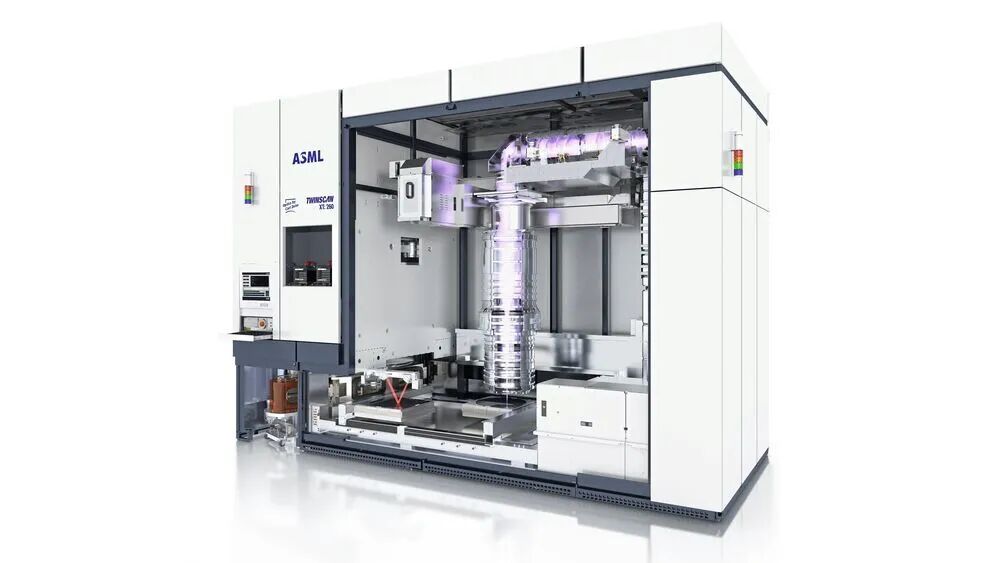
The TWINSCAN XT:260 launched by ASML last year is an i-line scanner that can process 270 wafers per hour. In view of the growing demand for AI chips, ASML plans to shift its business focus from pure front-end chip production equipment to packaging and bonding technologies in the next 10 to 15 years. (Image source: ASML)
But ASML is obviously not satisfied with only providing advanced packaging lithography equipment.
In March this year, South Korean media The Elec reported that ASML has started the overall architecture design of hybrid bonding equipment and has been in contact for cooperation with long-term suppliers such as Prodrive Technologies and VDL ETG. These enterprises previously participated in the supply of precision motion systems, drive devices and mechanical structures for ASML's lithography equipment. If ASML tries to transfer its accumulation in high-precision motion platforms to bonding equipment, it may further narrow the technical distance between lithography equipment and hybrid bonding equipment.
Moreover, there is another point worthy of attention that ASML has already published related patents.
The international patent WO2026098870A1 published on May 15, 2026 is titled "Bonding Apparatus", with the applicant being ASML Netherlands BV. The patent relates to a bonding device for two semiconductor substrates, focusing on discussing how to improve the alignment problem that may occur in the bonding process through state control of the substrate support surface. The patent document points out that factors such as internal stress of the wafer, support surface state and flatness may cause alignment deviation during bonding. This is obviously related to ASML's long-term research on wafer deformation compensation, position measurement and precision motion control technologies.
Of course, patent layout does not mean that mass-produced equipment is already mature. ASML has not yet publicly confirmed the commercial delivery time, customer certification progress or mass production performance of its hybrid bonding equipment. But this potential competition has begun to affect the market's expectations for traditional equipment enterprises. On October 6, Bank of America downgraded Besi's investment rating, which mentioned the competitive risk that ASML may enter the hybrid bonding market in the future.
For Besi, this risk is worthy of attention. In the traditional advanced packaging equipment market, Besi's important advantages come from long-term accumulation in precision mounting, assembly processes and hybrid bonding technology. Once ASML officially enters, it may form a new competitive force with its experience in nanoscale positioning, precision measurement and large-scale complex equipment system engineering.
However, from having key technical capabilities to developing competitive commercial equipment and then passing the mass production certification of wafer fabs, there is still a considerable long process of technology and commercialization.
Whether ASML can really challenge Besi ultimately depends on the alignment accuracy, throughput, yield, equipment stability, cost and customer certification progress of the equipment, and cannot be judged solely based on patents or supply chain news.
Why Has Hybrid Bonding Become the Focus of Competition?
An important background for front-end equipment giants to enter advanced packaging one after another is that chip interconnection technology is changing.
In traditional 2.5D and 3D packaging, chips usually establish electrical connections through Micro-bumps. Thermal Compression Bonding (TCB) achieves reliable connection between solder and metal pads by applying temperature and pressure. This process is widely used in the field of high-performance computing and memory chips, but with the increase of chip stacking layers and the improvement of interconnection density, traditional micro-bump structures are gradually facing higher requirements in terms of pitch, connection height, parasitic effect and thermomechanical reliability.
Hybrid bonding provides another technical route. It combines direct dielectric bonding with metal interconnection to reduce the dependence on traditional solder bumps, thus making it possible to achieve smaller interconnection pitch, higher connection density and more compact chip stacking structure.
In May 2026, Imec, the Belgian microelectronics research center, and EV Group announced that they had achieved a 200nm copper interconnection pitch in wafer-to-wafer hybrid bonding research. The research team achieved a post-bond copper pad overlay deviation of less than 40nm for all test chips on 300mm wafers.
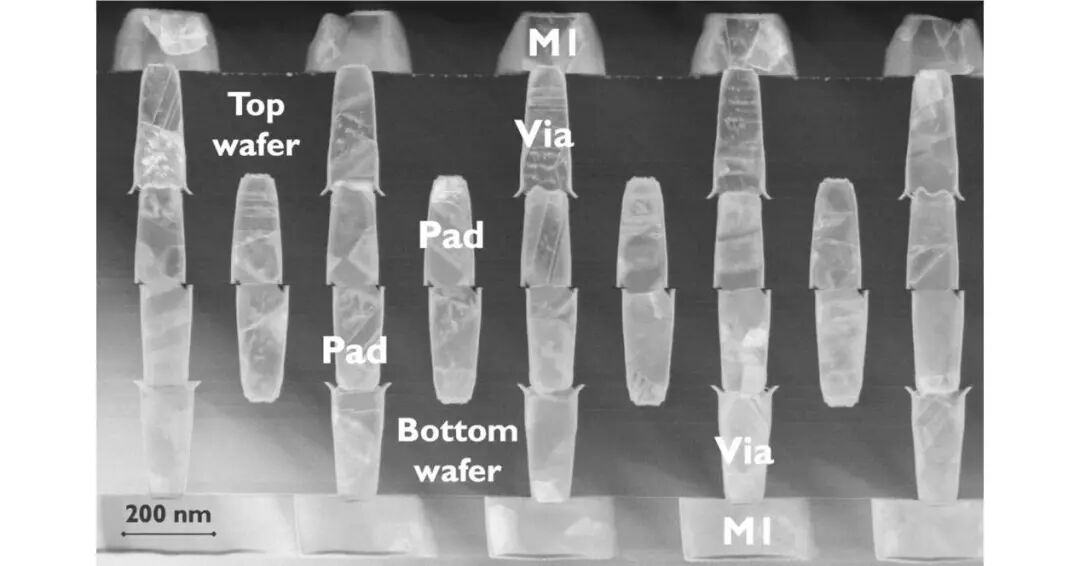
Transmission electron microscope image of the daisy chain structure on a 200nm hexagonal pad grid with hybrid pads of the same size and 25% designed copper density. (Image source: imec/IEEE)
Imec also emphasized in related research that in addition to alignment accuracy, surface topography control brought by CMP,