The AI frenzy is shaking up the semiconductor industry.
The explosion of AI computing power is reshaping the demand logic of the global semiconductor industry. As the iteration cost of advanced processes continues to rise, Chiplet heterogeneous integration and advanced packaging have become key technologies to improve the performance of computing chips. Large AI models drive the large-scale construction of intelligent computing infrastructure, and the evolution of power supply architecture, high-speed interconnection, and high-density integration force the synchronous iteration of upstream components and equipment. China's semiconductor industry has also bid farewell to the stage of prototype R&D, with many new products taking mass production and delivery as well as client adoption as their core goals.
On October 14, the 2026 Bay Semiconductor Expo officially opened in Shenzhen. With an exhibition area exceeding 70,000 square meters, this expo gathers more than 1,000 high-quality enterprises across the industrial chain from over 20 countries and regions around the world, covering four core links: wafer manufacturing, compound semiconductors, advanced packaging, IC design and AI infrastructure, with a number of new technologies and new products making their global debut. Throughout the exhibition, AI has become the common development direction targeted by all product lines at this event.
Power supply is the infrastructure of computing power, and power semiconductors take the lead in exploring new development paths
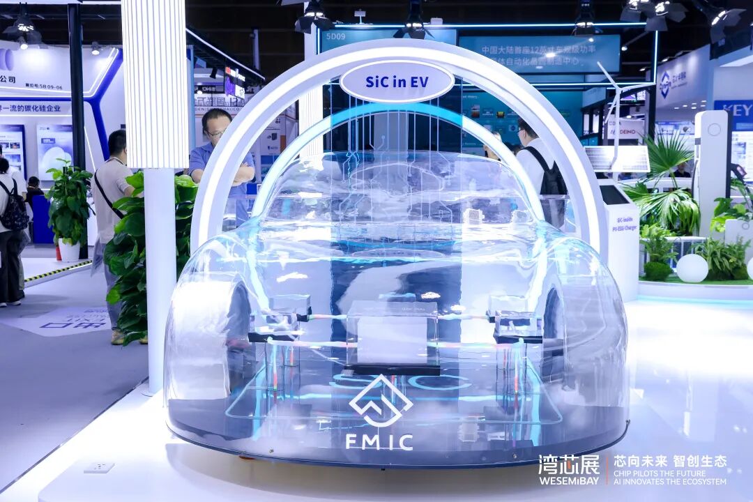
At this Bay Semiconductor Expo, the exhibits of power semiconductor manufacturers still focus on mature and market-oriented solutions. Main drives for new energy vehicles, on-board power supplies, photovoltaic energy storage, and industrial power supplies remain the mainstream application scenarios of exhibits. A large number of automotive-grade SiC MOSFETs and power modules are delivered for mass production, industrial-grade wide-bandgap devices have completed multi-specification iteration, and the localized implementation in traditional application markets continues to advance. Among them, Founder Microelectronics launched the SiC DIP32 power module, debuting two products of 1200V 35mΩ and 1200V 60mΩ, equipped with self-developed automotive-grade chips, and has passed the 3000-hour reliability test. It features high withstand voltage margin and strong high-voltage shock resistance, with small parameter drift under high temperature and stable performance. The standardized integrated solution can reduce wiring and debugging, providing a compact and reliable SiC power solution for the three core on-board power systems.
At the same time, the new market demand spawned by AI computing power infrastructure has become a brand new variable that draws high attention from the whole industry. Many exhibiting enterprises placed their data center power supply solutions at the core of their booths, and solid-state transformers (SST) have become a frequently mentioned technical keyword.
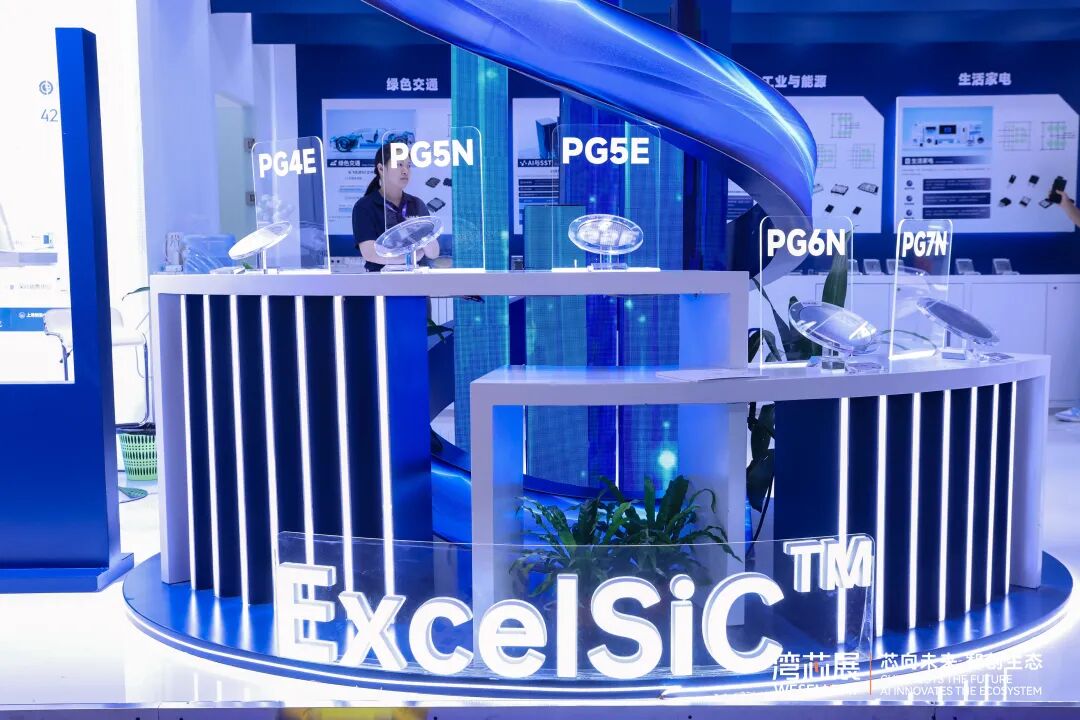
To adapt to the application scenarios of AI data centers, Yangtze Advanced launched discrete devices as well as EZ2C and EZ3C featured module products based on the PG4E chips that have achieved mature mass production, effectively improving the operating efficiency of server power supplies and reducing the overall power cost. The enterprise also demonstrated its technical layout in various application scenarios of AI power supply, providing SiC discrete devices and modular packaging solutions from 650V to 3300V, compatible with hard switching, soft switching and resonant topologies. According to on-site staff, after adopting SiC MOSFET, SST is mainly adapted to the operating frequency of 50 kHz - 100 kHz, which is much higher than the operating frequency of traditional IGBT. Higher operating frequency can greatly reduce the volume of the transformer. Moreover, SiC MOSFET has lower on-resistance under the same high-voltage specification, significantly reducing high-frequency operation loss, no need to configure high-power heat dissipation components, and further improving the system response speed. Although GaN devices, which are also third-generation semiconductors, have excellent high-frequency performance, mature commercial products mainly cover the voltage range below 650V, with insufficient reliability under high-voltage working conditions above 1200V, which cannot meet the requirements of high-voltage scenarios.
In addition to SST, in the evolution process of the high-voltage DC architecture of AI data centers, solid-state circuit breakers adapted to the 800V DC architecture are also a key research direction of the industry. Traditional mechanical circuit breakers have difficulty in breaking on the DC side, while solid-state circuit breakers use semiconductor devices to achieve microsecond-level breaking. NVIDIA has clearly recommended the use of solid-state circuit breakers for distribution loop protection in its 800V DC architecture white paper. The main switch of solid-state circuit breakers requires devices to conduct normally, turn off quickly at the moment of failure, and withstand large current shocks, which is exactly the capability range of normally-on SiC JFET: it conducts at zero gate bias, suitable for carrying main current for a long time; its specific on-resistance is about half of that of MOSFET of the same specification, and the conduction loss is close to that of mechanical circuit breakers; the bulk conduction structure and avalanche characteristics make it more robust to withstand overload and short-circuit shocks.
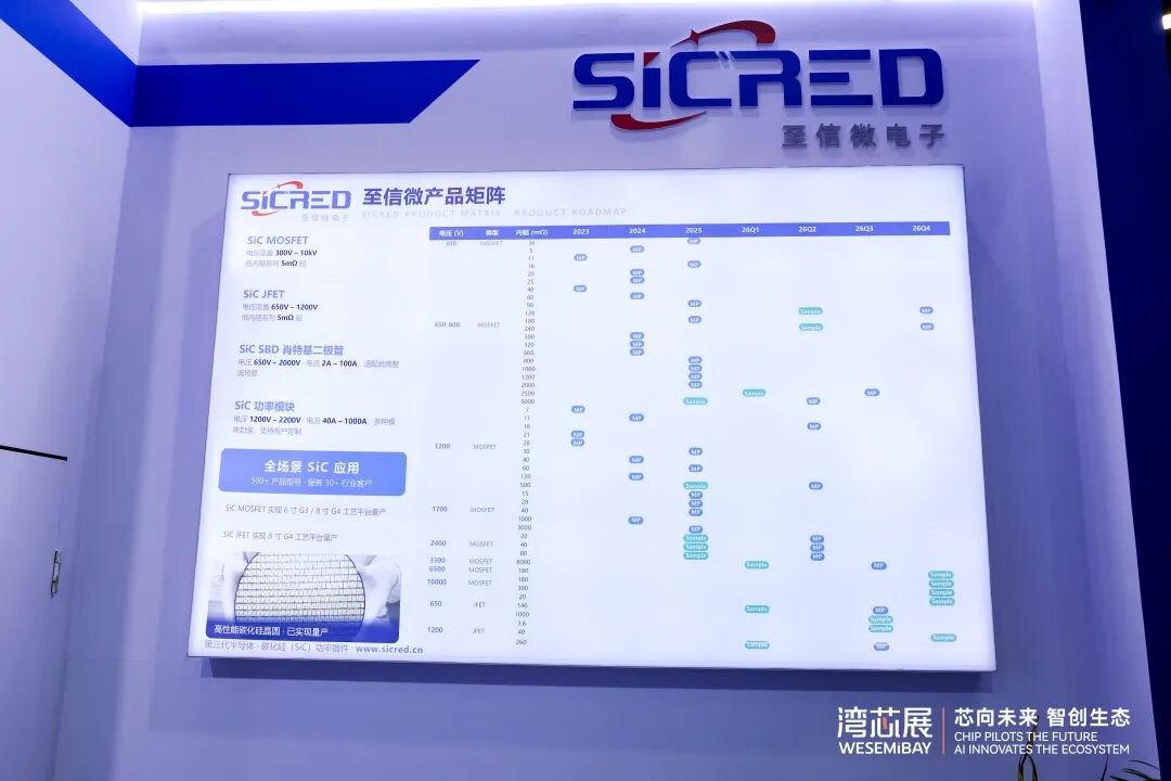
At this exhibition, Zhixin Microelectronics exhibited a series of SiC JFET product solutions, including multiple specifications of 650V (20mΩ, 140mΩ, 1000mΩ on-resistance) and 1200V (3.6mΩ, 40mΩ, 260mΩ on-resistance). At present, this series of products has achieved mass production relying on the 8-inch G4 process platform. According to the staff, Zhixin Microelectronics is the first manufacturer in China and the third in the world with the mass production capability of JFET-structure silicon carbide. Previously, only ON Semiconductor and Infineon in the world had relevant mass production capabilities, among which ON Semiconductor has the most complete product line. Zhixin Microelectronics said that the JFET product launched by the company has an on-resistance as low as 3.6 mΩ, which is unique in the world, and the on-resistance of similar overseas products is generally concentrated in the 20-40mΩ range. It was learned on site that other domestic silicon carbide manufacturers have also started the R&D and mass production layout of JFET devices, and it is expected that more domestic products will be launched to the market in 2027.
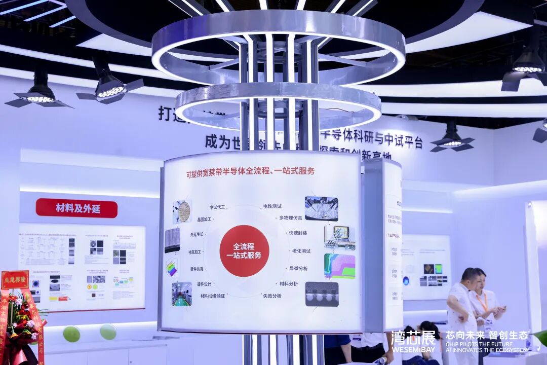
The implementation of mass production and delivery is supported by the underlying R&D links. For cutting-edge devices, enterprises focus on sample and mass production verification, while the underlying process, material and reliability challenges can be fully undertaken by public R&D platforms. At this Bay Semiconductor Expo, Shenzhen Pinghu Laboratory demonstrated the platform capabilities including material epitaxy, pilot test center, analysis and testing center. The laboratory has built a pilot test platform without heavy metal pollution, which can complete the whole front-end process of 8-inch non-silicon semiconductors without heavy metals such as gold, silver and copper, providing necessary conditions for the pilot R&D of high-performance and high-reliability power devices and non-silicon integrated circuits.
Semiconductor equipment targets advanced processes, advanced packaging and storage tracks
The industrial transformation brought by AI not only acts on the chip products themselves. The continuous expansion of the shipment scale of computing chips directly drives the simultaneous capacity expansion of wafer manufacturing, storage and advanced packaging; with the construction of production lines taking the lead, equipment procurement has become the primary investment for capacity expansion, and the equipment link has also become the industrial chain link that directly undertakes AI demand. At this Bay Semiconductor Expo, a number of new semiconductor equipment products were unveiled intensively.
Huahai Qingke released the medium-beam ion implanter IHQ-900E. According to the introduction, this product is the first domestic medium-beam ion implanter with performance exceeding that of foreign competing products. It leads foreign competing products in some key indicators such as dose uniformity, angle, Dose Rate, Beam Current and WPH. It is equipped with a self-developed software platform of Huahai Qingke, with the domestic localization rate of the whole machine reaching 95.6%, and it is expected to achieve full localization in 2027.
SEARI Equipment released the Venus 6 series advanced packaging metrology and inspection equipment, which is the first domestic equipment that can simultaneously carry out multi-process synchronous metrology and inspection for TGV (Through Glass Via) and RDL (Redistribution Layer) of large-size glass substrates in the semiconductor advanced packaging process. The product has multi-modal synchronous inspection integration technology, supporting a variety of extended functions (compatible with panel-level and wafer-level substrates, 3D morphology measurement, infrared imaging inspection).
Micro-D Nano launched the brand new iMagtron series magnetron sputtering system (PVD) and the special ALD equipment for Ru ultra-thin film process, realizing full-system coverage of the three mainstream thin film deposition technology routes of ALD, CVD and PVD. The iMagtron series magnetron sputtering system has a more compact overall size (reduced by about 10%), leaving enough maintenance space; it adopts a modular design, and the same system meets different process requirements of Cu1-Cu4 for different applications and technology nodes. In terms of overall process, for various application pain points such as optimized design of Ta/TaN, the PK Life time is optimized by more than 50%. The special ALD equipment for Ru process of the iTomic MeT series atomic layer deposition system can realize the formation of continuous Ru thin film of less than 5nm on various substrates through atomic-level nucleation regulation technology, with key indicators reaching the mass production reference level.
Tuojing Technology released the amorphous carbon thin film deposition technology Flowable Carbon. Flowable Carbon has been applied to the NF-300M Supra-H equipment. This technology series stably realizes two flowable carbon film processes with different filling properties through the selection of precursors and the control of process conditions, namely Capi-Carbon and Sedi-Carbon. Tuojing Technology has carried out cooperation with 3D-NAND, DRAM and logic chip manufacturing enterprises around the above two flowable carbon film deposition technologies, aiming at the actual structural and process requirements of customers to solve special problems in applications, and continuously expand the application scenarios of carbon film technology.
Xinhui Equipment focused on demonstrating the latest progress of seven businesses: crystal growth, thin film deposition, grinding and thinning, polishing micro-processing, optical metrology, chemical metrology, and chip testing. As a key layout track, Xinhui Equipment exhibited products such as the XV1280 automated storage test machine. The XV1280 is oriented to the wafer-level CP test requirements of NAND storage chips, supporting high-parallel testing and flexible configuration, with a maximum of 1280 DUTs tested simultaneously. It is understood that its storage test equipment has been delivered more than 200 units in total.
Aixin Semiconductor fully demonstrated four product lines: optical wafer metrology, X-ray wafer metrology, advanced packaging metrology and inspection, and high-end scientific instruments. Among them, the HYI series is the star product, with cumulative shipments of more than 100 units, and the HighYield IM300 machine of this series was also brought to the site. The HYI series can seamlessly connect with process equipment such as CMP and etching, complete high-precision metrology of optical thin films and critical dimensions, realize real-time process monitoring, and meet the control requirements of advanced process technologies.
The value of advanced packaging is highlighted, becoming an important support for AI chip performance
The performance of AI chips is highly dependent on advanced packaging technologies, and the industrial status of the packaging and testing links has been greatly improved accordingly. This Bay Semiconductor Expo has a dedicated exhibition area for advanced packaging, covering Chiplet heterogeneous integration, 2.5D/3D packaging, wafer-level packaging, TSV, glass substrates and packaging materials.
Huatian Technology demonstrated advanced packaging solutions such as HFCBGA, FCBGA, 3D FAN OUT SiP, FoCS (2.5D Chiplet) and SiCS (2.5D Chiplet). Among them, FCBGA and HFCBGA both belong to the FC flip-chip technology route. Products with 70×70mm specification have achieved mass production, and it is expected that mass production of 110×110mm ultra-large size products will be completed in 2027. The staff said that traditional packaging products are mainly ordinary BGA and simple power device packages, which are mature businesses that are not hotspots in the market. The unit price of products is extremely low, generally priced at the level of cents, mao or li, and the price of a single product is mostly below 1-2 yuan, with extremely low overall profit space and no long-term growth potential. However, the value of a single large-size high-specification advanced packaging product can reach more than 1000 yuan, with very considerable profit space, which is the core layout direction of current packaging manufacturers. At present, Huatian Technology has invested about 4 billion yuan in Nanjing to build an advanced packaging factory, focusing on advanced packaging technologies such as FC, 2.5D and 3D packaging.
AI ecosystem has an independent exhibition area, domestic computing power is accelerating its implementation
In addition to packaging, testing and equipment, AI chips themselves also have clear landing points at this Bay Semiconductor Expo. This Bay Semiconductor Expo has set up the AIE AI Infrastructure Industry Ecosystem Exhibition Area for the first time, and a number of representative AI chips and computing power manufacturers participated in the exhibition with related products and solutions.
Lanxin Computing Power demonstrated the world's first RISC-V+AI intelligent convergence server CPU — LX500 and full-scenario computing power products covering data centers, high-performance intelligent computing, university scientific research, finance, government and enterprise and other fields, focusing on demonstrating the integrated mass production results of "Chip - Complete Machine - Ecosystem". According to the introduction, the LX500 main frequency covers 2.0GHz-2.3GHz, with a design upper limit of 2.9GHz, including 32 general-purpose cores and 16 AI inference cores, and the computing power of a single chip is 75 TOPs. The staff said that the relevant standards for large RISC-V chips were officially implemented in 2023, which is only 3 years ago, and the industry is currently in the early stage of concentrated outbreak of finished products.
Jiangyuan Technology fully demonstrated the full-stack computing power products including self-developed AI chips, AI acceleration cards, intelligent computing all-in-one machines, and intelligent computing servers, building a complete product system from underlying core chips, boards and cards to desktop AI terminals and enterprise-level intelligent computing equipment. Its first-generation D1 GPU chip focuses on pure inference scenarios, equipped with LPDDR5X video memory, and the dual-chip co-packaging solution can double the computing power, which has now achieved mass production. The second-generation T1 chip adopts HBM video memory, supports integrated inference and training, with a video memory bandwidth of 4.8T/s, and has completed tape-out verification. The D20 high-performance acceleration card based on self-developed GPU chips has a single card power consumption of 145W, video memory configuration of 64G/128G, and its computing power is comparable to NVIDIA H2. The D20 16-engine intelligent computing server displayed on the booth can deploy 16 self-developed D20 acceleration cards in the 4U chassis space, and the whole machine can provide 1024GB/2048GB local video memory. On-site staff explained that the full configuration of 16 acceleration cards has extremely high requirements for the number of PCIe channels of the processor, so it needs to be matched with a specific Intel dual-CPU model; domestic Haiguang and Phytium CPUs can currently support a maximum of 8-card deployment.
This Bay Semiconductor Expo is like a microcos