The chip consumes too much power! What should we do?
In modern data center chips, power delivery has become a critical bottleneck restricting performance scaling. The surge of artificial intelligence (AI) and high-performance computing (HPC) workloads has posed severe challenges to the power delivery network (PDN) that far exceed the design capabilities of traditional solutions. As current levels rise, the resistive loss and voltage droop effects in the PDN intensify, and incremental improvements alone can no longer meet the demand. Stacked-die multi-chip architectures further exacerbate this problem, as they lead to increased effective current density, routing congestion, and reliability challenges.
Recently, Intel released a white paper exploring power delivery challenges at all levels from accelerators, racks to data centers, with a focus on how scaling trends are reshaping power requirements across the entire system hierarchy. This article does not advocate for a single "optimal" power delivery solution. Instead, it outlines a series of technical approaches that senior architects and technical experts can selectively apply based on system requirements and architectural tradeoffs.
Power Delivery Challenges for Chips
Design trends in the chip, server, and data center domains are pushing power delivery capabilities to their physical limits. As compute density increases, to maintain robust power integrity (PI), the entire power delivery network (PDN) must be optimized across all layers from the circuit board, packaging to the silicon die.
Accelerator Packaging Design Trends
Modern accelerator packages integrate unprecedented computing, storage, and interconnection resources in a single package to meet the performance and bandwidth requirements of artificial intelligence (AI) and high-performance computing (HPC) workloads.
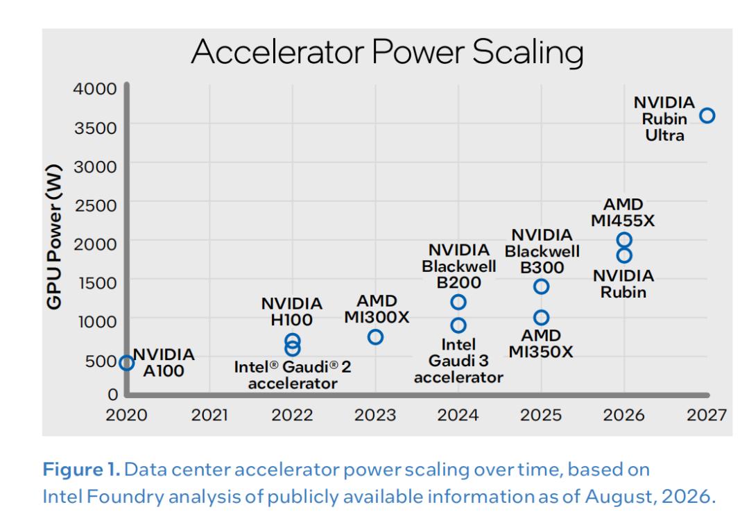
AI accelerators typically operate at low supply voltages and require large currents to deliver high power (see Figure 1). As a result, modern levels of integration require package-level currents on the order of thousands of amperes (kA). These trends give rise to two fundamental power delivery challenges.
First, the package must deliver enormous power within a limited footprint, an area already occupied by compute dies, high-bandwidth memory (HBM) stacks, high-speed interconnects, and thermal management infrastructure. Second, the power delivery process must be highly efficient while minimizing both static and dynamic losses in the power distribution network (PDN).
Delivering high currents efficiently is extremely challenging, especially when voltage conversion is located far from the load. Current must travel through long resistive paths, which increases resistive losses and reduces overall power delivery efficiency. In addition, higher currents and faster transient changes exacerbate voltage droop, forcing designers to set voltage guard bands to ensure reliable operation. These guard bands increase power consumption and further reduce system efficiency.
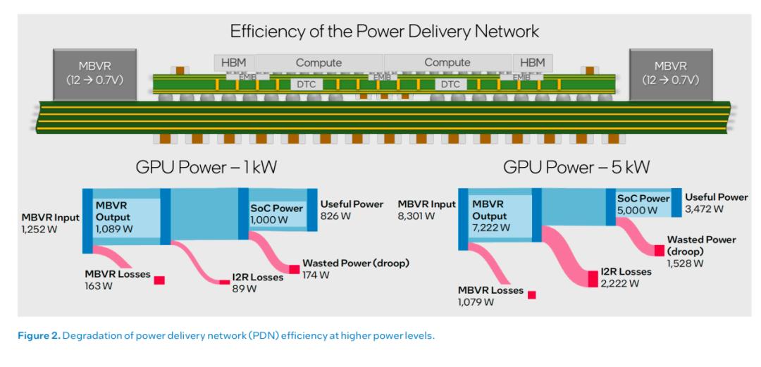
Figure 2 shows how PDN efficiency decreases as load current increases. While voltage conversion losses remain relatively constant, resistive losses and losses associated with voltage droop increase significantly at high power levels.
As a result, for traditional power delivery schemes, the proportion of input power consumed by the PDN is growing, while the proportion of effective power actually used for computing is correspondingly reduced.
Multi-Chip and Stacked Architectures
As traditional single-die scaling faces increasingly severe economic and technical challenges, the industry is turning to advanced packaging technologies — including chiplets, HBM integration, silicon bridges, and 3D stacking — to continuously improve system-level performance and bandwidth. While these multi-chip and stacked architectures deliver higher performance, bandwidth, and functional integration, they also introduce new challenges for power distribution, decoupling, and voltage regulation.
Unlike traditional monolithic designs, multi-chip architectures distribute computing, storage, and I/O functions across multiple silicon dies, each with distinct requirements for voltage, current, and transient response. Power must be delivered to each individual die through a variety of packaging structures such as interposers, silicon bridges, package substrates, microbumps, and through-silicon vias (TSVs). At the same time, the operating voltage margins for HBM interfaces and die-to-die interconnects are increasingly tight, and they are highly sensitive to power supply noise.
The growing complexity of heterogeneous accelerator packages also brings challenges to the silicon wafer itself. The integration of compute tiles, memory interfaces, and high-speed die-to-die links places increasing pressure on signal routing resources. In traditional front-side power delivery architectures, power rails and signal interconnects must share routing resources, leading to a fundamental tradeoff between signal bandwidth and power delivery capability. To support ever-increasing signal density, advanced technologies continue to add routing layers and adopt increasingly complex interconnection structures.
However, these additional routing layers can also increase the effective resistance of power delivery paths, as current must pass through more vertical interconnection layers before reaching the active circuits. Under high current conditions, this extra resistance leads to greater IR drop, lower power delivery efficiency, and further compressed voltage margins.
These trends are driving a fundamental architectural shift toward backside power delivery technology, which moves the power distribution network to the backside of the wafer, freeing up signal routing resources on the front side and reducing the resistance and routing congestion issues inherent in traditional power delivery networks (PDNs).
Data Center Power Trends
The increase in per-rack power is reshaping power delivery requirements and imposing strict constraints on footprint, thermal dissipation, and architecture. Traditional data center racks typically have a design power of 10 to 20 kilowatts (kW), relying primarily on air cooling and leaving ample space for power supplies, cables, and airflow management. In contrast, modern artificial intelligence (AI) racks have exceeded 100 kilowatts, and liquid cooling has been widely adopted to cope with the resulting heat flux. The increase in rack power density not only reduces the available space for power conversion, distribution, and cooling infrastructure, but also raises the energy efficiency requirements for the entire power chain.
Looking ahead, industry roadmaps predict that rack power will approach 1 megawatt (MW) later in this decade; this means that space efficiency, loss minimization, and tight coupling of power delivery and cooling systems will no longer be optional, but essential design requirements.
The design premises of data centers have changed dramatically over the past decade. According to estimates from Lawrence Berkeley National Laboratory in June 2026, by 2030, data centers in the United States may consume 11.8% of the country's total electricity consumption (the specific proportion depends on the scale of AI deployment and infrastructure assumptions, with an expected range of 9.5% to 15.3%). This forecast is higher than the estimate in the 2024 report, which predicted that data center electricity consumption would account for 6.7% to 12.0% of total U.S. electricity consumption by 2028 — the main driver of this growth is the surge in demand for high-density computing in AI and accelerator-based devices.
At the same time, as the deployment scale of high-power accelerators continues to expand, power delivery and thermal management infrastructure face increasingly severe challenges, while device technology roadmaps continue to push package power levels higher. GPUs are one of the main engines driving the growth of AI workloads, bringing higher power consumption while boosting computing performance. Higher power levels lead to disproportionate efficiency losses and pose severe thermal management challenges. These issues drive up operating costs and cooling demands, and increase infrastructure complexity. Therefore, improving end-to-end power delivery efficiency has become increasingly critical for future large-scale expansion.
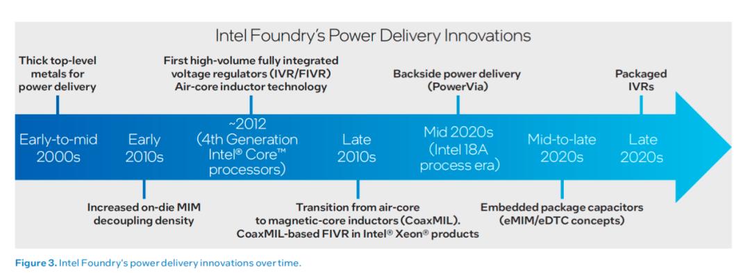
Many of the power delivery challenges faced by today's AI accelerators first appeared in Intel's high-performance CPUs; on these chips, growing current demands pushed traditional power delivery architectures to their limits. Figure 3 shows how Intel addressed this challenge through a series of pioneering power delivery innovations that were later widely adopted across the industry. These include thick metal layers for improved power distribution, the introduction of on-chip metal-insulator-metal (MIM) capacitors, and early forms of integrated voltage regulators (IVRs).
The power consumption demands of modern AI accelerators are driving innovation in a new generation of power delivery technologies. To address these challenges, Intel Foundry is advancing multiple technologies, including backside power delivery, advanced package-level decoupling solutions, embedded bridge technology using through-silicon via (TSV) technology, and a new generation of IVR architectures that move power conversion closer to the load. These technologies are explored in detail in the following sections.
Backside Power Delivery: Separating Power and Signals
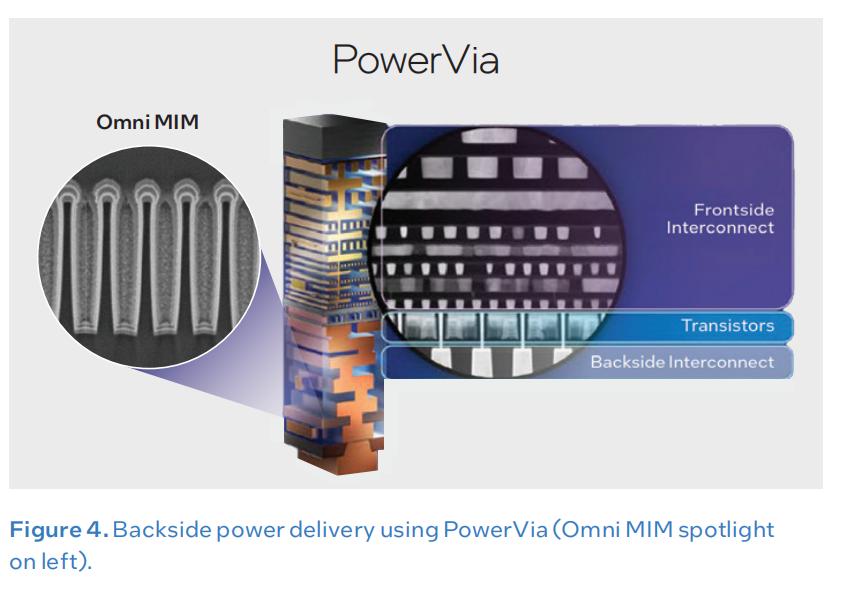
In traditional front-side power delivery architectures, power rails and signal interconnects compete for the same routing resources, leading to a fundamental tradeoff between signal bandwidth and power delivery capability. As the complexity of the metal layer stack increases, current must pass through more routing layers before reaching the transistors, resulting in greater IR drop. Power Via technology reroutes the main power supply to the back side of the chip, physically separating power routing from front-side signal interconnects (see Figure 4). This approach shortens the resistive current path, alleviates front-side routing congestion, and allows both networks to be independently optimized.
Power Via technology can significantly reduce on-chip IR drop, make more efficient use of front-side routing resources for signal transmission, and improve standard cell utilization. For high-current logic circuits, backside power delivery directly addresses many of the fundamental scaling limitations of traditional front-side power delivery networks (PDNs).
To realize these advantages, close collaborative optimization across multiple levels including process integration, thermal management, and architectural design is required.
PowerVia technology was first introduced on the Intel 18A process, and also laid the foundation for Power Boost on Intel 18A-P; Power Boost is an all-new dual-contact architecture that delivers over 10% frequency improvement while maintaining the same capacitance. PowerDirect is Intel Foundry's second-generation backside power delivery technology planned for the Intel 14A process. It inherits the advantages of PowerVia, and further improves area efficiency and optimizes power delivery architecture to comprehensively improve power, performance, and area (PPA) metrics.
Omni MIM: On-Die Decoupling Capacitors
While backside power delivery minimizes on-chip IR drop, achieving robust power integrity also requires improved on-die decoupling technologies to support the large transient currents generated by AI workloads. Intel pioneered the introduction of MIM (metal-insulator-metal) capacitors into mass-produced logic processes, providing on-chip capacitance to meet high-frequency decoupling requirements.
The close-up view on the left side of Figure 4 shows Omni MIM, Intel Foundry's latest generation of on-die MIM capacitor technology. Early MIM capacitors adopted planar structures, and subsequent generations increased capacitance density by adding more electrode layers. While this approach worked, the improvements it delivered were limited to incremental gains, as capacitance increases roughly linearly with the number of plates. Omni MIM takes a different approach, extending the capacitor structure into the third dimension. By introducing vertical trenches in the interlayer dielectric, Omni MIM achieves a significant increase in capacitance density while remaining in close proximity to the active circuits.
eMIM-T and eDTC: Advanced Package Decoupling Solutions
On-die MIM capacitors are the first line of defense against fast current transients. However, their stored charge is limited and must be supplemented by the next level of decoupling capacitors. Traditionally, this role has been filled by discrete ceramic capacitors mounted on the land side and die side of the package. In high-density accelerator packages, the top area is almost entirely occupied by compute and memory dies; at the same time, the land side is densely populated with ball grid array (BGA) connections to support high-current power delivery and off-package I/O transmission. This leaves very limited space for traditional surface-mount decoupling capacitors, highlighting the importance of embedded capacitor technologies.
Intel Foundry is developing two complementary embedded capacitor technologies to meet these needs:
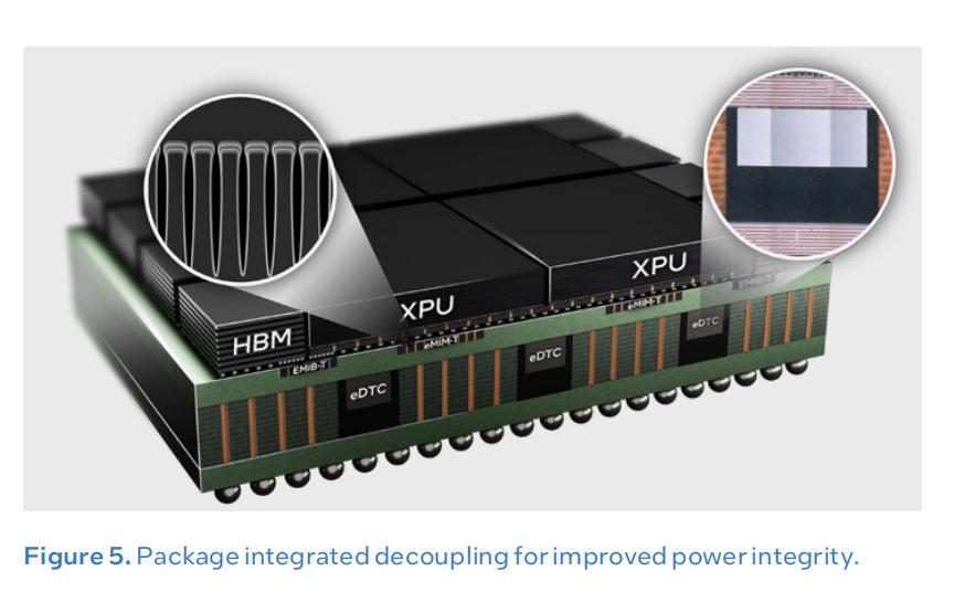
Intel Foundry's proprietary eMIM-T capacitor technology extends Omni MIM technology into the package, integrating multiple layers of high-density MIM capacitors in the package build-up layers (see Figure 5). By placing capacitors closer to the load, eMIM-T improves high-frequency decoupling performance while using through-silicon via (TSV) connections to maintain DC power delivery. In designs where on-die capacitance is limited by area or process constraints, the eMIM-T structure can supplement on-die charge storage functionality without consuming valuable silicon area.
Embedded deep trench capacitors (eDTC) are integrated inside the package to provide an additional level of decoupling capacitance, maximizing the total capacitance within the package and helping to meet decoupling requirements in the low to mid frequency range.
EMIB-T: Enabling HBM4 and High-Speed Die-to-Die Interconnects
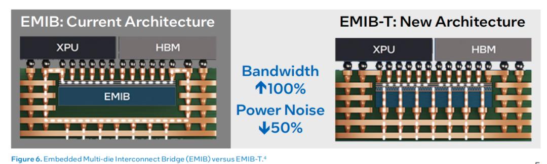
The embedded multi-die interconnect bridge (EMIB) shown on the left side of Figure 6 is an advanced packaging technology from Intel Foundry that enables multi-chip architectures without the use of a full silicon interposer, avoiding the associated high cost and complexity.
Since its introduction in 2017, EMIB has played a key role in enhancing the bandwidth and die-to-die interconnect capabilities of advanced multi-chip packages. As AI and HPC platforms adopt high-bandwidth interfaces such as HBM4 and next-generation Universal Chiplet Interconnect Express (UCIe) links, current demands also increase. In traditional EMIB implementations, power paths have to route around the bridge structure, which increases path resistance. As current density rises, IR drop increases and can cause current crowding at edge bumps.
This raises concerns about energy efficiency and reliability.
The newer EMIB-T architecture, shown on the right side of Figure 6, addresses these limitations by integrating through-silicon vias (TSVs) directly inside the bridge structure. These TSVs provide a more direct vertical current path to the load, allowing current to pass through the bridge structure rather than routing around it. This not only reduces resistive losses, but also distributes current more evenly across the bump array, helping to mitigate reliability risks for edge bumps.
EMIB-T also integrates MIM capacitors within the bridge structure for local suppression of alternating current (AC) noise on high-speed I/O power rails. Combined, these features provide more robust power delivery for next-generation high-bandwidth chiplet architectures.
At the IEEE/JSAP Symposium on VLSI Technology held in June 2026, TSMC introduced its first angstrom-class CMOS platform, along with its backside power delivery solution.
According to the introduction, this node combines enhanced nanosheet gate-all-around transistors and backside power delivery technology. Its key integration feature is the Super Power Rail (SPR), which TSMC describes as a backside direct contact power delivery scheme designed to meet the demands of applications such as artificial intelligence and high-performance computing with dense power networks and complex signal routing. Compared with N2P technology, A16 technology delivers 8% to 10% higher speed at the same power consumption, or reduces power consumption by 15% to 20% at the same speed, while increasing chip density by 8% to 10%, and is expected to enter mass production in the fourth quarter of 20