Enterprise Case Sharing: Yupan Liangzhi - Engineering Practice of Ion Trap Quantum Computing Chip Integration | 36Kr 2026 Industry Future Conference
The 2026 Industrial Future Conference focuses on opportunities in the new cycle, and jointly explores the future of industries and the birth of "Light of China". Zeng Ruqi, Executive President of Yupan Quantum Intelligence, focused on the theme of engineering implementation of quantum-intelligence integration for ion trap quantum computing, and thoroughly dissected the core challenges, technical paths and industrial logic for this technical route to expand from laboratory settings to large-scale deployment. As industrial investment enters the deep-water zone where capital, technology and industries are accelerating their integration, how can quantum computing complete the leap from "scientific device" to "computer"? Yupan Quantum Intelligence provides the answer of advancing the engineering of quantum-intelligence integrated computing via semiconductor industrial methodologies.
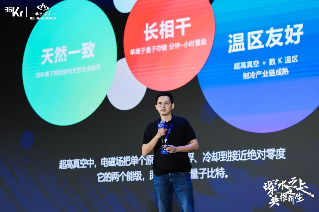
Speaker: Zeng Ruqi, Executive President of Yupan Quantum Intelligence
Zeng Ruqi: Dear guests and peers, hello everyone! It is a great honor to have this opportunity to share my insights with you all.
Today I want to talk about a very specific issue: if ion trap technology is to step out of the laboratory, what engineering challenges will we encounter, what work are we doing at present, and why do we choose to carry out this work in Yizhuang?
01 Ion Trap: From "Single High-Quality Qubit" to "Large-Scale Computer"
Ion trap is one of the mainstream technical routes that have been verified in engineering by the current industry, and is widely recognized to have the potential to lead to large-scale general-purpose fault-tolerant quantum computing.
The so-called ion qubit is a charged atom suspended in an ultra-high vacuum by an electric field, which encodes quantum information by selecting specific energy levels of the atom.
Its unique advantages come from a simple fact: its qubits are natural atoms in essence.
In terms of engineering implementation, this starting point brings three values:
▍ Naturally consistent qubits.
The physical properties of any type of atom in nature are completely identical, which means the consistency and repeatability of qubits are naturally guaranteed by the laws of physics; as a result, ion qubits do not have nanoscale manufacturing errors that exist in solid-state devices, which means we do not need to perform separate calibration and compensation for each qubit. Although in real systems, calibration of system parameters such as local magnetic field, driving intensity, electric potential and motion mode is still required, it significantly reduces the engineering complexity caused by device discreteness after scaling up.
▍ Long coherence time.
Ions naturally have excellent quantum coherence characteristics; according to public literature, the quantum storage time of a single ion under specific experimental conditions can reach the order of minutes or even hours. The longer the coherence time, the larger the time window reserved for quantum logic operations, feedback control and quantum error correction, which is also an important reason why ion traps are very suitable for the development of high-fidelity computing and fault-tolerant quantum computing.
▍ Friendly operating conditions.
Ion qubits do not rely on a dilution refrigeration environment close to absolute zero, and can operate at room temperature. For lower noise, higher vacuum quality and control electronics integration, the current operating system mainly adopts a low-temperature vacuum platform environment of several Kelvin, and the corresponding vacuum and refrigeration equipment supply chain is already very mature in China.
However, the real challenge of ion traps does not lie in "whether a single qubit performs well".
When the system continues to expand from hundreds of qubits to a larger scale, the real difficult problem becomes: how can so many ion qubits with excellent performance truly form a computer that can run stably and efficiently for a long time?
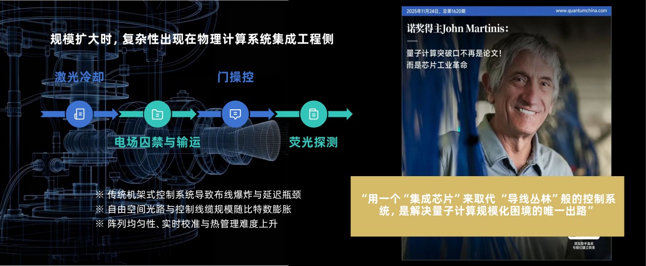
John Martinis, winner of last year's Nobel Prize in Physics, once put forward an important view: quantum computing also needs to experience its own industrial revolution. In essence, it means gradually evolving from scientific devices in laboratories to computing systems based on semiconductor industry that can be manufactured, replicated and continuously iterated.
For ion trap technology, this means that the key is no longer "how many qubits can be demonstrated at present", but how to gradually integrate the quantum physical computing system that was previously scattered on large optical platforms, electronic instruments and vacuum systems into chips and quantum-intelligence systems, so as to solve a series of engineering problems such as wiring explosion, noise, synchronization, time delay and complex control after the scale expands.
▍Scalable expansion from "single stage" to "assembly line": QCCD architecture
To make a large number of ion qubits work collaboratively, the first question to answer is "how to organize them". There is a very important architecture for ion trap scaling up — QCCD (Quantum Charge-Coupled Device).
Its core idea can be simply understood as: instead of squeezing more ions into a long chain to complete all calculations, the physical computing system is divided into different functional areas, such as storage area, quantum logic operation area, readout area, loading area and ion transport channels. During calculation, corresponding ions are moved to the designated area to complete specific operations through electric field control.
To make an engineering analogy: it is equivalent to splitting an increasingly large "single stage" into a large number of standardized "workstations" and "assembly lines". Each local area is kept in a small-scale state that is easy to control, and then a large-scale quantum physical computing system is formed on the whole through ion transport and system scheduling.
This is also the core architecture direction that Yupan has chosen.
▍After QCCD, the real difficulties are just beginning
QCCD solves the first layer of problem of "how to organize a large number of ions". However, as the ion scale continues to expand, new engineering problems will arise immediately: how to transport ions quickly? How to drive a large number of electrodes? How to wire an increasing number of control channels? How to synchronize different areas? How to complete real-time feedback? How to calibrate the whole system automatically?
Therefore, further realizing the deep integration of quantum chips, proximal control electronics and classical computing systems on the basis of QCCD architecture has been the focus of industry research in recent years.
In February this year, the team from the Technical University of Brunswick in Germany published their work in JSSC, which is a representative of this engineering trend: further integrating the electronic system for ion qubit control into the chip level in the low-temperature zone.
The founder of Yupan was invited to participate in the engineering technical guidance of relevant German projects in 2023, and we are one of the earliest R&D teams in the industry engaged in the research of QCCD proximal control electronics integration.
02 Develop ion traps with semiconductor methods: Yupan Quantum Intelligence's engineering practice
"Yupan" (which means jade disc) is like a "semiconductor wafer". What Yupan Quantum Intelligence is doing is to build a supercomputer with "native quantum-intelligence integration" using semiconductor industrial methods.
Our team is built with "engineering implementation" as the core orientation. The founder is a national-level talent in the field of quantum integrated chips. The team covers three directions: integrated circuits, quantum physics and advanced computing. Most of the core team members have a background in microelectronics engineering research. From January 2024 to today, we have completed the tape-out verification of multiple chips including low-temperature quantum measurement and control, ion trap QPU, and cross-temperature zone quantum interconnection, and we will launch a prototype based on our self-developed chips next year.
Our goal is not to "build a larger scientific experimental device", but to bring quantum computers into the semiconductor industrial production line, and make a chip-level integrated quantum-intelligence computing system that can be taped out, replicated and continuously iterated.
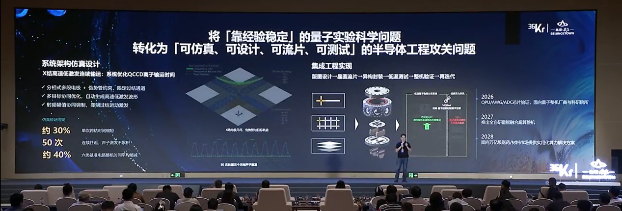
In other words, what we are doing is to gradually transform the quantum experimental scientific problems that used to rely heavily on the experience of experimental personnel into engineering research problems that "can be simulated, designed, taped out and tested".
▍A specific example: How do ions pass through the "intersection"
Take the optimization of a very typical problem in QCCD — "ion transport" which takes up a lot of time in quantum physical computing as an example.
In a large-scale QCCD system, the execution of quantum algorithms not only includes the quantum gate itself, but also a large number of ion movement, junction crossing, rearrangement and possible re-cooling processes. In some algorithms and system configurations, these operations will take up a considerable part of the execution time, and gradually become an important factor limiting the operating efficiency of the system.
Especially after QCCD develops from a one-dimensional structure to a two-dimensional structure, ions need to pass through cross structures such as X-junctions frequently, and the importance of transport efficiency will become higher and higher. In the classic design, a junction crossing process usually consists of multiple segmented transport processes, and it is also necessary to take into account the speed, ion stability and final state motion excitation.
Our idea is : instead of treating "passing through an intersection" as several isolated steps, we systematically define and design the whole junction crossing process as a complete two-dimensional continuous dynamic problem.
Through system dynamics simulation, we directly optimize the multi-channel voltage waveforms between different electrodes, so that ions can complete the cross-junction transport continuously along the designed trajectory, and control the final state motion excitation at the same time. Under the current model and constraints, the simulation results show that there is significant room for improvement in the cross-junction efficiency, and the relevant work results are being submitted for publication.
The real value of this work is not only that the simulation theory verifies "how much the single-pass speed increases". More importantly, we have established a complete link from "ion trap system simulation verification" to "real chip design requirement definition", which is our understanding of engineering implementation.
On the basis of completing system index design, performance simulation and chip structure definition, our microelectronics engineers can take over and realize chip manufacturing and system integration through semiconductor industrial methods.
▍ Engineering innovation of ion trap QPU chip-level integration
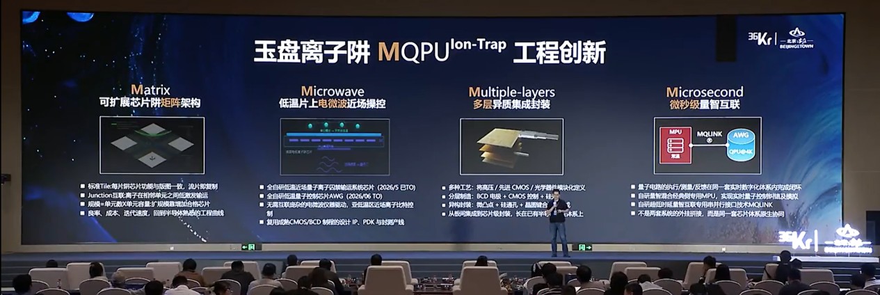
The engineering innovation of our ion trap QPU is mainly reflected in four aspects:
① Modular scalable architecture
On the basis of QCCD architecture, we use highly consistent semiconductor technology to make different ion trap functional units into standardized modules, and realize ion path switching between different regions through X-junctions and high-speed transport channels.
In this way, the subsequent growth of ion qubit scale no longer fully relies on re-designing the single chip, but can rely more on standard module replication, chip manufacturing consistency, high-speed ion transport and system-level scheduling.
Modularization will not eliminate routing, congestion and control complexity in large-scale systems, but it can structurally decompose the originally highly coupled problems, making system scale expansion more manageable.
② Near-field microwave quantum manipulation
The manipulation of classic ion trap systems relies heavily on free-space optical paths. Our approach is to gradually transfer the expansion pressure of the "quantum coherence manipulation" layer, which has extremely high requirements for stability, to the near-field electronic control system based on self-developed electric microwave chips. We are not trying to eliminate lasers completely. The cooling, state initialization and detection of ions still require optical systems, and we are also promoting the modularization and integration of these optical parts.
The really important engineering significance of near-field microwave quantum manipulation is that electric microwave chips have a very mature industrial foundation in frequency synthesis, waveform generation, chip integration, large-scale manufacturing and long-term stable operation.
Once problems such as near-field microwave high gradient field generation, crosstalk, thermal management and local addressing can be solved through chip-based integration, it will provide an engineering implementation route for the large-scale expansion of ion qubits that can be based on the current semiconductor industrial foundation.
③ Heterogeneous integration with layered manufacturing
According to the characteristics of different modules of the ion trap operating system, we select different semiconductor processes for engineering implementation. We have completed tape-out verification of multiple processes such as micro-nano, high voltage, advanced CMOS, and silicon photonics. Different modules are taped out separately, the electronic performance is tested, and then the quantum system is integrated and tested: from inter-PCB integration to heterogeneous integrated chip packaging.
The greatest value of this engineering implementation is that there is no need to wait for a dedicated semiconductor process line to be fully mature at present, but to use the existing semiconductor production line to complete the integrated engineering implementation that the industry has not done before.
④ Cross-temperature zone real-time interconnection
For large-scale quantum physical computing systems, and for the future integration of quantum and intelligent computing, we must also solve a large number of I/O, cross-temperature zone wiring and high-speed data transmission problems at the system level.
If each control channel is directly connected from the room temperature zone to the low-temperature quantum chip with an independent cable, as the scale expands, the number of cables, thermal load, number of interfaces and system complexity will increase rapidly. Therefore, while promoting the integration of low-temperature measurement and control chips, we are also developing MQLink, a dedicated high-speed interconnection chip technology for quantum-intelligence system interconnection.
Through the high-speed serial interface, we can significantly reduce the number of cross-temperature zone cables, increase the data bandwidth per physical connection, and establish a deterministic, low-latency digital transmission path.
What it solves is not simply "transmitting data faster", but: how to maintain a manageable number of I/O, high bandwidth, deterministic latency and strict synchronization between the scaled qubits and the classical computing system.
This is essential for the implementation of real-time feedback and fault-tolerant quantum computing.
03 Chip-level quantum-intelligence integrated design, facing the essential bottleneck challenge of "effective computing power"
Yupan is one of the very few computing companies in the industry that starts from the quantum-intelligence integration architecture layer, and puts the self-development of classical AI dedicated computing processors and quantum processors on an equal footing. Our self-developed dedicated AI computing ASIC MPU (Memory-centric Process Unit) is about to complete tape-out. Based on MPU, the dedicated quantum-intelligence interconnection chip MQLink, and the chip-based measurement and control integrated ion trap QPU, we will soon launch the MQPU computing system with native quantum-intelligence integration design featuring architecture-level innovation.
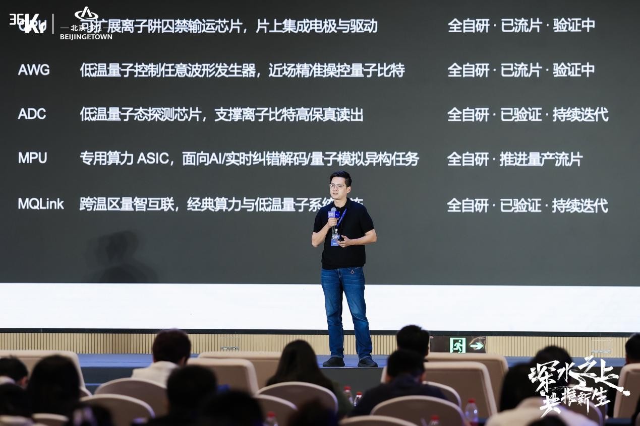
▍Quantum-intelligence integration requires breakthroughs in chip-level integrated architecture innovation
At present, the physical layer of multi-route quantum computing has completed engineering verification. The mainstream prototype verification computing systems generally connect multiple sets of systems such as CPU, GPU, FPGA, measurement and control instruments and low-temperature quantum physical computing systems through general interfaces. The more this integration mode moves towards large-scale deployment, the more obvious the bottlenecks become: wiring explosion, excessive delay, synchronization difficulties, and complex orchestration, which fundamentally restrict the "effective