Jen-Hsun Huang's three assertions have all backfired, and the moat of CUDA has been pierced through by just one line of code from Google.
Just now, SemiAnalysis released the first third-party inference performance measurement of Google's 7th-generation TPU Ironwood.
Under fully equivalent model loads, the TPU delivers up to 50% higher performance per dollar than NVIDIA B200, and its lead over B300 is even close to doubling at 96%!
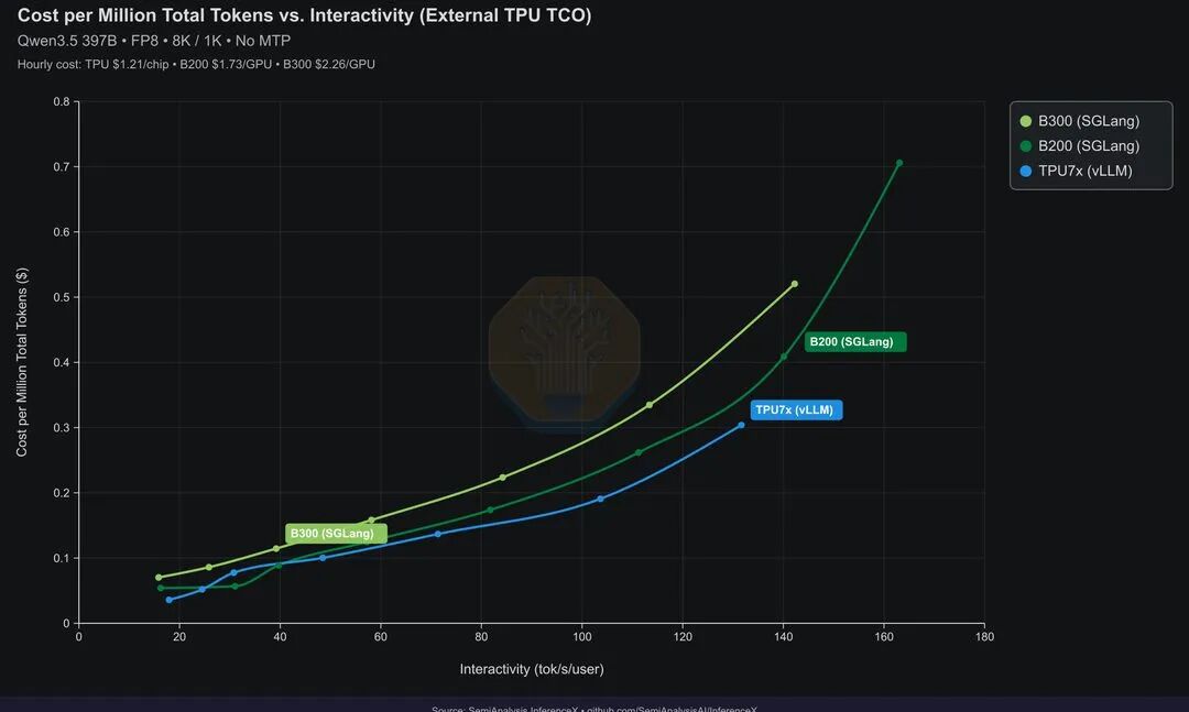
Cost per million tokens vs. interaction speed under external TCO standard
Converted to the most industry-sensitive metric of cost per million tokens, the gap is staggering.
The TPU only costs $0.181, the B200 costs $0.222, and the B300 is as high as $0.276.
What's even more dramatic is the timeline.
Back in April this year, Jensen Huang claimed on the Dwarkesh Podcast that neither TPU nor Trainium dared to run benchmark tests. He even publicly encouraged challengers to use InferenceMAX to prove their so-called inference cost advantage.
Five months later today, the TPU arrives as promised with game-changing data.
Jensen Huang's Three Assertions
In that podcast episode, Jensen Huang's strategic contempt for TPU can be summed up in three assertions.
First, he stated that he was extremely eager to see competitors prove TPU's cost advantage, and insisted that this was logically impossible to establish at all.
The test method this time is completely fair and impartial —
The same open-source model, FP8 vs FP8, 8k input and 1k output, the B200 and B300 run exactly the same load as the TPU.
At the single-user throughput benchmark of 100 tokens per second, TPU is 19% cheaper than B200 and 34% cheaper than B300.
If the median response time is capped at 20 seconds, the TPU costs $0.098, the B200 costs $0.106, and the B300 soars to $0.132.
The B200 does not lose all metrics. It still maintains a slight resistance within the narrow interval of 30-second response time. But as latency requirements are relaxed, TPU regains its leading position.
As for the B300, it is at a cost disadvantage throughout the entire process.
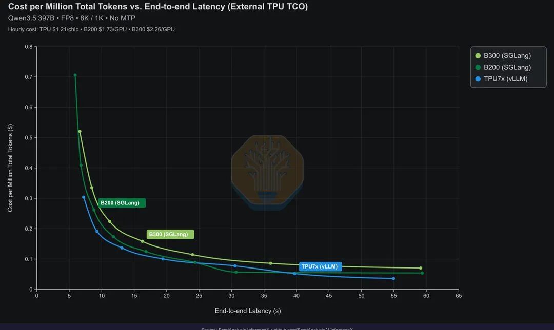
Cost per million tokens vs. end-to-end latency
Second, he claimed that from the first principles, TPU's advantages are completely unjustified.
Physical tests did not overturn his underlying deduction, Jensen Huang just miscalculated the accounts in the business world.
In most intervals of the original throughput curve, the physical performance of TPU is indeed inferior to that of GPU. But the hourly rental cost of TPU is drastically lower.
A 5% physical throughput advantage combined with extremely low unit-time rent instantly translates into a 50% cost-performance advantage per dollar.
If calculated based on Google's internal bottom-line cost of $1.03 per chip per hour, this advantage will be amplified to 77% or even 130%.
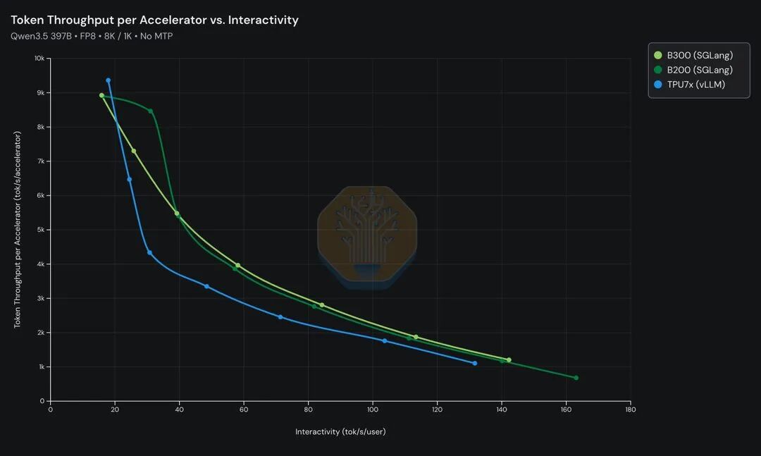
Single accelerator throughput vs. interaction speed
Jensen Huang calculates the absolute computing power squeezed out by a single chip, while business customers measure the actual output that can be purchased with every dollar.
This publicly released benchmark data directly breaks through the psychological defense line of customers.
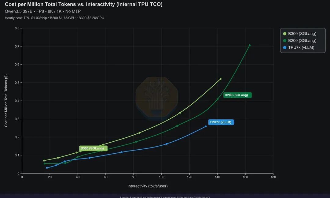
Google internal TCO standard
Third, he concluded that Anthropic is just a special case, and TPU will completely lose its growth engine without Anthropic's support.
This assertion currently only holds true on the surface.
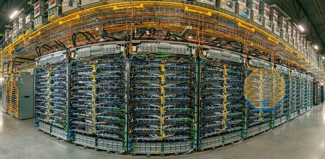
Anthropic has indeed deployed more than 1 million TPUs, of which about 400,000 are purchased directly and 600,000 are leased through Google Cloud. By 2029, it will surpass DeepMind to become the world's largest single user of TPUs.
But the other half of the assertion is quickly becoming invalid.
Google has opened up direct chip sales since last year, no longer sticking to the single model of cloud leasing. Even researchers inside DeepMind now need to compete for computing resources in a crowded queue.
Jensen Huang dared to say so in April because TPUs had never been priced publicly before.
Now the price tag is out, and it is marked by someone else on behalf of Google.
The Deep Water Zone of TPU's Cost Advantage
How on earth can a dedicated chip achieve cost suppression over general-purpose GPUs?
In this regard, SemiAnalysis reveals Google's completely different engineering philosophy at the underlying logic level —
Google never pursues the physical peak of a single chip, but casts the computing die, inter-chip interconnection and underlying compiler into a closed-loop system, squeezing costs at every joint.
At the chip level, Ironwood is physically split into two independent computing dies, each embedded with 2 TensorCores and 4 SparseCores.
Its HBM capacity reaches 6 times that of the previous generation Trillium. This number directly determines how large the KV Cache can be and how large the Batch can be set.
It is also the first generation of TPU that natively supports FP8 operations, completely saying goodbye to the software simulation compromises of several previous generations.
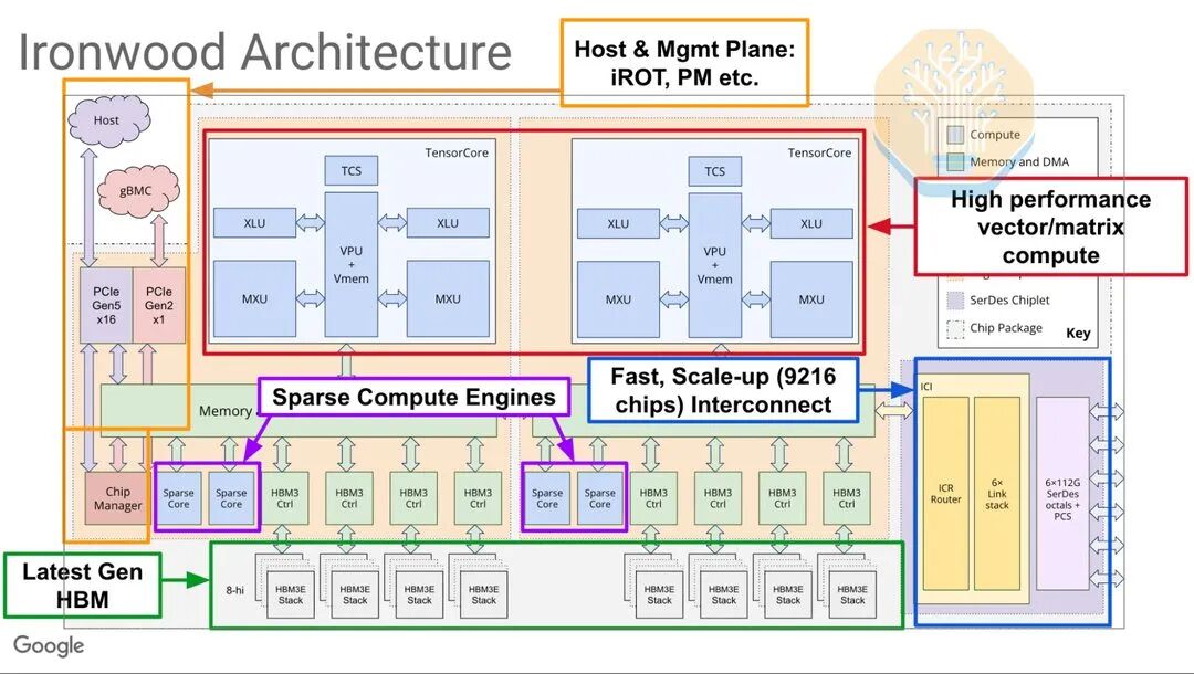
The matrix unit adopts a 256×256 systolic array, completing 65536 multiply-accumulate operations per cycle, and the computing throughput directly soars to 4 times that of the v5 architecture.
This route is even more extreme in the 8th generation: Google for the first time splits training and inference into two chips 8t and 8i. The on-chip SRAM of 8i is expanded to 384MB, 3 times that of the previous generation, which is specially used to store the KV Cache of inference models on the chip.
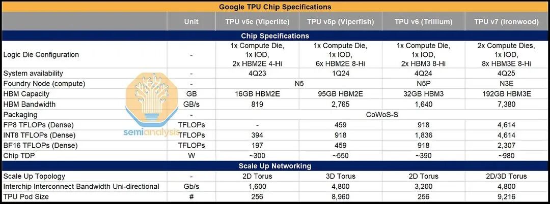
Comparison of specifications of all generations of Google TPU
In terms of network interconnection, chips directly exchange data through Google's self-developed ICI bus, completely bypassing the host CPU, PCIe and general network cards.
Its topology is in a 3D Torus form, each chip is physically connected to 6 adjacent nodes, 64 chips form a rack-level cube, and then spliced through optical circuit switches all the way to a super matrix of 9216 chips.
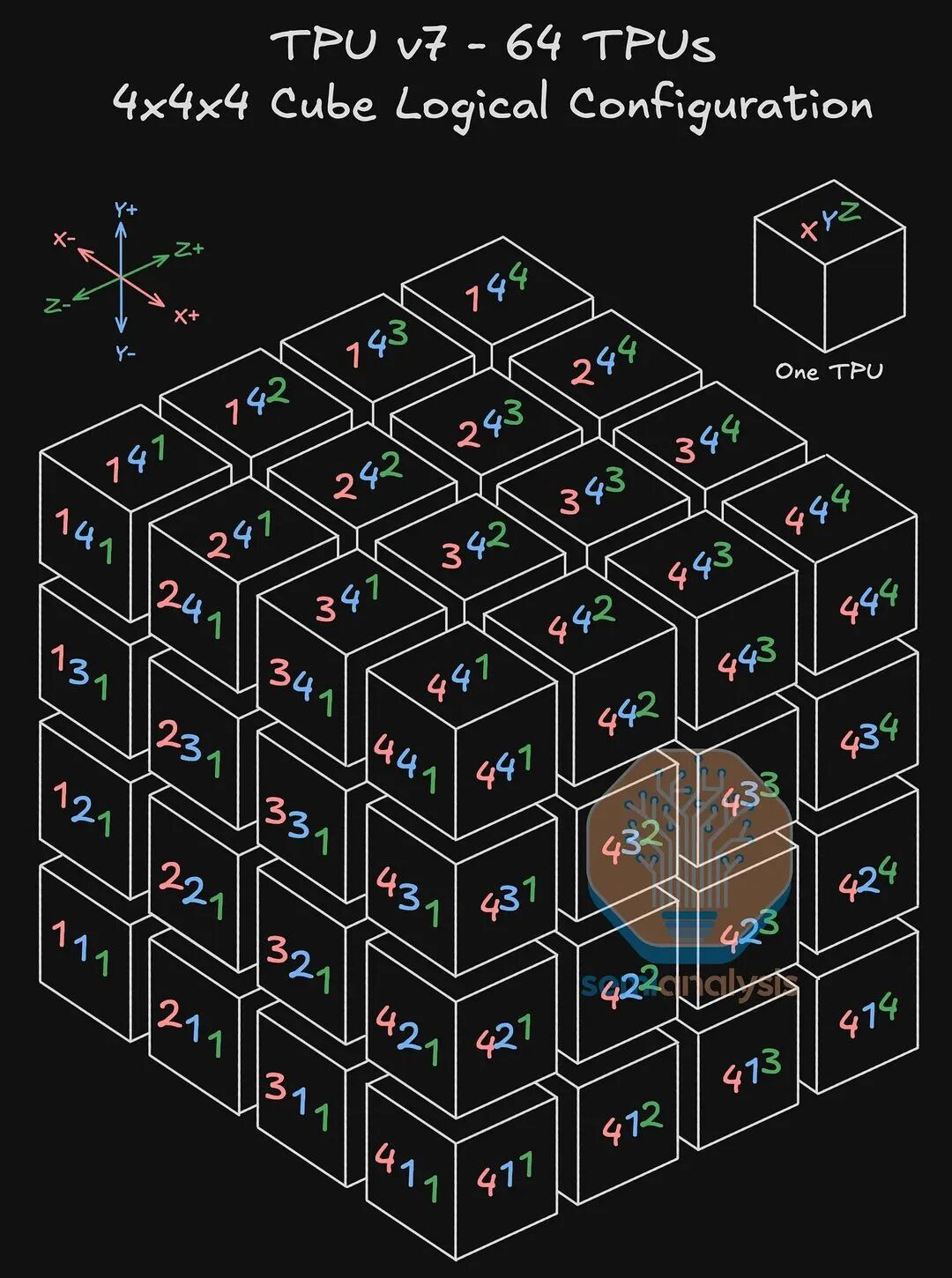
4×4×4 cube logical configuration of TPU v7
If any optical fiber link fails, the system can use the optical mirror to complete rerouting within a few seconds without manual intervention.
For TPU 8i, 3D Torus will be replaced with the Boardfly topology, the maximum hop count at the scale of 1000 chips is reduced from 16 to 7, and the tail latency accumulated by each hop in MoE routing and multi-turn Agent scenarios is directly cut in half.
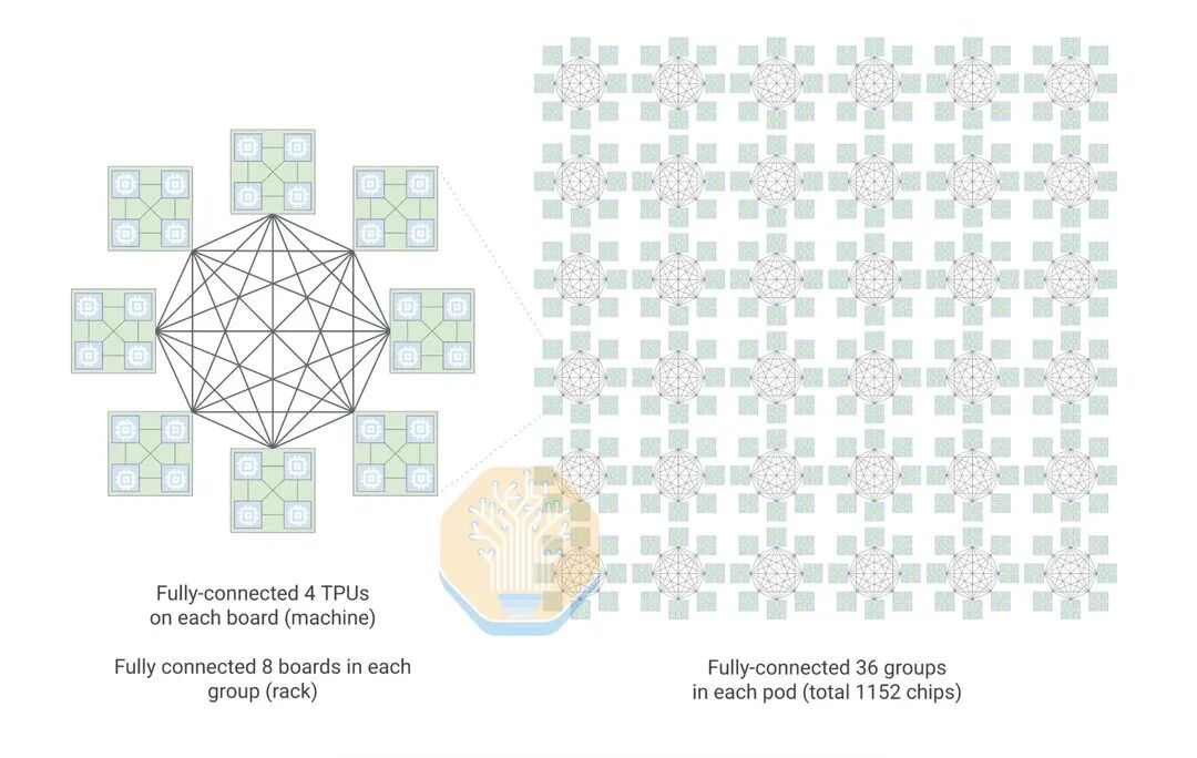
Boardfly topology of Google TPU 8i
Code-level Refactoring That Delivers 50% Performance Gain
Extreme performance is often hidden in the brute-force refactoring of underlying software.
To get the first model on the TorchTPU stack to run smoothly, Google, Inferact and RadixArk jointly invested hundreds of engineering hours.
By digging into a large number of code commit records, three decisive optimizations can be extracted.
First, doubling the number of KV Cache pages to greatly reduce the first token latency.
The tile processed by the TPU vector unit each time is hardware-locked to 128 lanes in the last dimension, and zeros will be forcibly padded if the dimension is insufficient.
The old attention kernel packs KV along the head dimension, resulting in half of the computing resources of models with single KV head being swallowed by invalid zero-padding operations.
Now Google moves the token to the 128-lane dimension, and the available KV pages surge from 5141 to 10283.
At a concurrency of 128, the throughput increases by 16.5%, the median first token latency drops sharply by 95%, and inference requests are completely free from the pain of queuing for KV space.
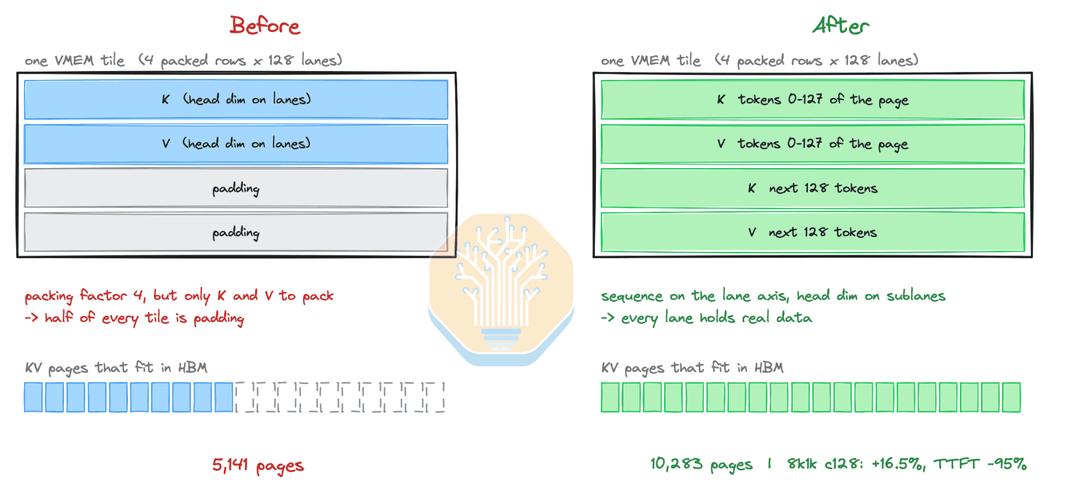
Comparison before and after KV cache layout transformation
Second, parameter decomposition to improve decoding throughput.
The page attention mechanism relies on double buffering to hide HBM latency, that is, prefetch the next block of data synchronously while calculating the current data.
The old heuristic algorithm locks both the calculation block and the read block to 16k tokens, resulting in no extra space in VMEM for prefetch operations.
Now the R&D team keeps the read block at 16k and reduces the calculation block to 4k, so that the decoding throughput jumps from 64.9k tokens per second to 96.3k.
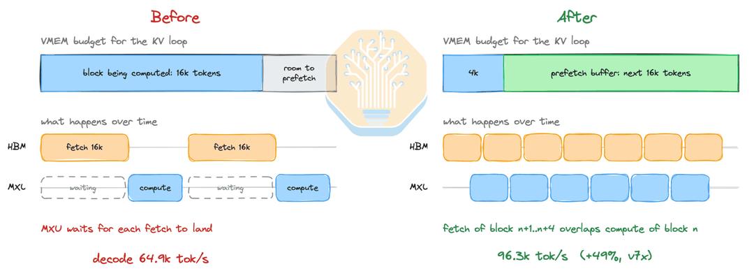
Before and after splitting the read block and calculation block
Third, transfer communication tasks to SparseCore.
The 4 SparseCores equipped on each Ironwood chip were originally dedicated to sparse calculations such as Embedding lookup.
Google transfers all ReduceScatter and MoE token rearrangement tasks to SparseCore, thus freeing up the computing resources of TensorCore to focus on core matrix multiplication.
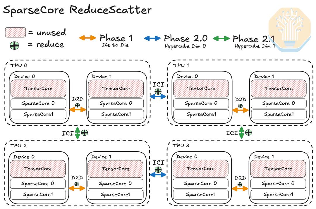
Three stages of ReduceScatter on SparseCore
Under the load of 8k input and 1k output, the throughput increases by 4.1% to 14.2%, and under the scenario of 1k input, 8k output and 512 concurrency, the throughput surges by 26.1%.
Hundreds of such tiny but crucial code optimizations are accumulated layer by layer, eventually creating this overwhelming 50% performance advantage.
Code-level Subversion That Fills the Ecological Moat
The most subversive part of this update is that Google only made changes to the software.
The entire open-source inference ecosystem was deeply rooted in the PyTorch and CUDA system before, while the native development environment of TPU is JAX.
Previously, to run vLLM on TPU, a translation layer called TorchAX was required to translate each operator to JAX for execution at the underlying level.
This translation layer caused a large number of compatibility issues with page attention and underlying optimizations