Apple's first 2nm smartphone chip has been released, introducing a brand-new packaging technology.
Apple has launched a brand-new top-tier system-on-chip for smartphones — the A20 Pro. This new processor made its debut at Apple's iPhone launch event held today, which is also the first launch event hosted by the new CEO John Ternus. A brand-new self-developed modem (C2) was also released at the same time.
A20 Pro is Apple's first 2-nanometer chip applied to iPhones. (Apple's first 2-nanometer chip is the M6, which the company released in August and will make its debut in the Mac Mini later this month.) Like the M6, the A20 is also equipped with a dual neural engine, brand-new CPU and GPU cores.
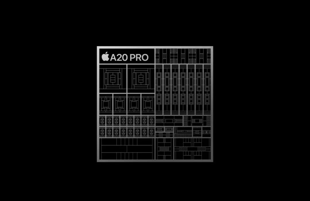
The A20 Pro will power the new foldable iPhone Duo, as well as the iPhone 18 Pro and Pro Max.
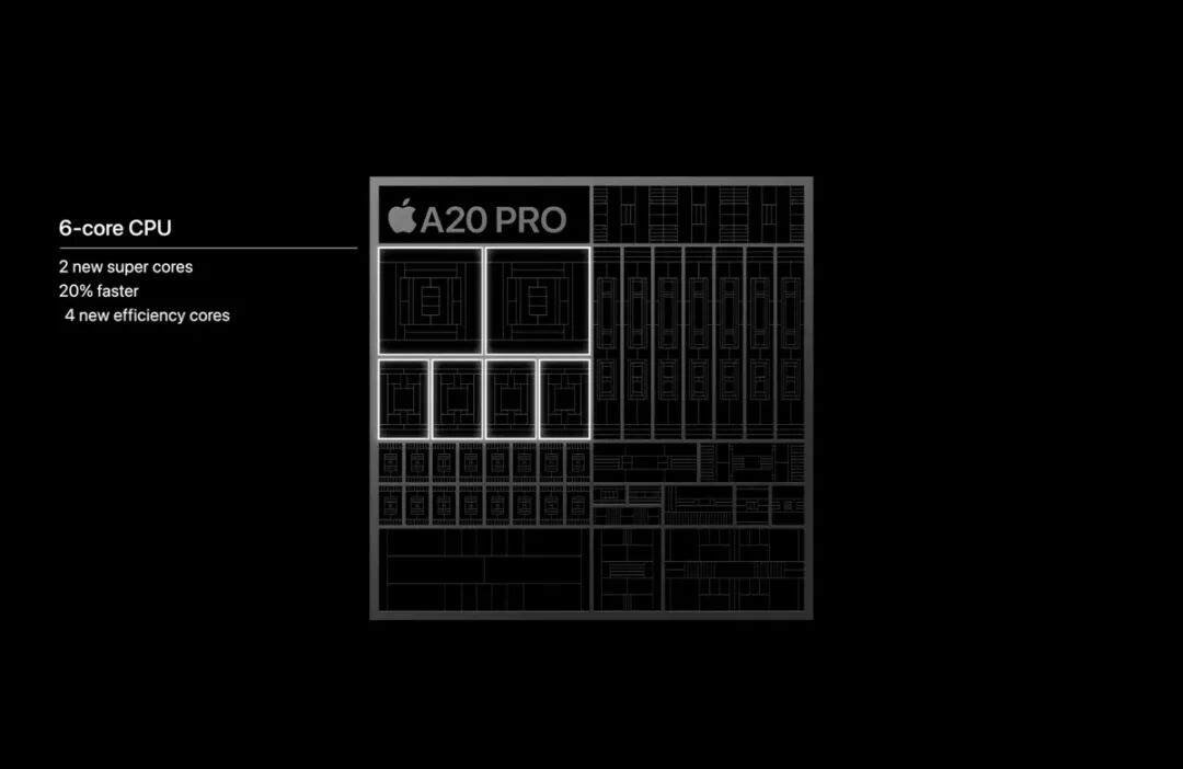
This brand-new SoC chip is equipped with a 6-core CPU, including two Apple performance cores that are 20% faster than the previous generation, plus four energy-efficiency cores with neural accelerators. Apple calls it a "desktop-class" processor and the "fastest CPU ever in a smartphone".
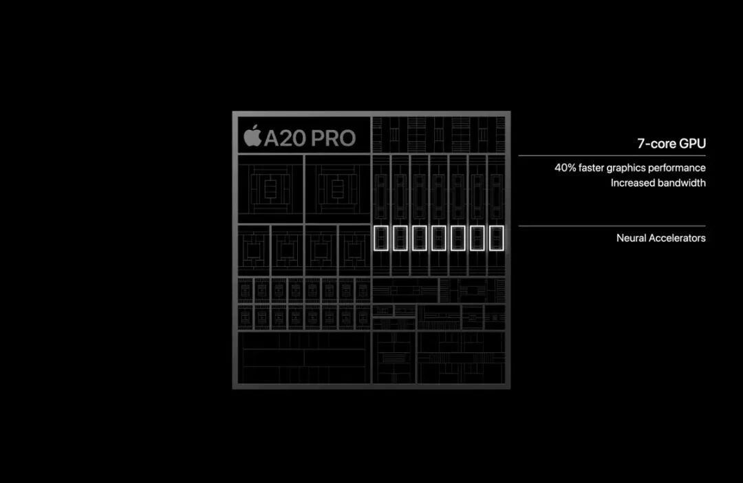
The performance of this 7-core GPU is 40% higher than that of the previous generation, with improved bandwidth, and it is also equipped with new neural accelerators, which the company says doubles the FP8 computing speed.
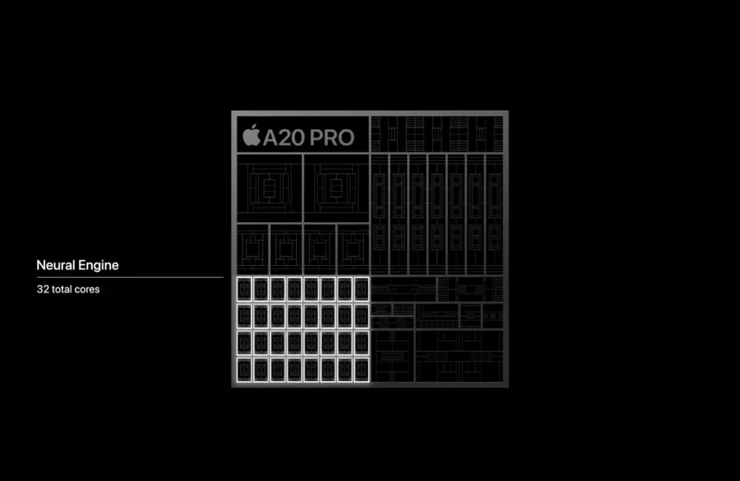
The A20 Pro also features a brand-new dual 16-core neural engine that accelerates on-device AI models and computational photography, with a total of 32 cores, delivering twice the AI processing capability of the A19 Pro. The chip's memory bandwidth has been increased by 50%, which Apple says is the chip with the widest memory interface in iPhones.
Apple has also improved the packaging method, placing the silicon chip away from the heat dissipation path of the SoC, so that the silicon chip can be directly connected to the vapor chamber. Compared with the 17 Pro, the surface area of this vapor chamber is tripled, and it uses more graphite and copper, as well as 80% recycled stainless steel.
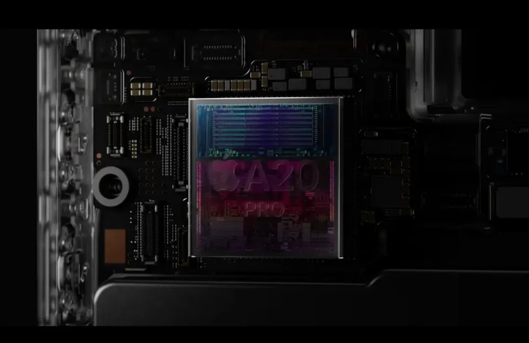
Apple introduced that the redesigned heat dissipation system is centered on a new generation of vapor chamber, whose surface area is three times that of the previous generation.
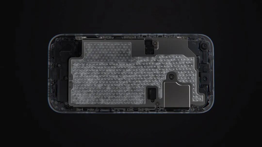
The brand-new vapor chamber continuously circulates deionized water, which significantly improves heat dissipation performance, allowing the A20 Pro chip to maintain higher performance for a longer time under high load.
Apple has redesigned the silicon packaging, adopting "customized packaging inspired by M-series chips" that places the silicon chip and memory side by side instead of stacking, thus removing the memory from the thermal path of the chip and allowing the A20 Pro to connect directly to the vapor chamber.
To achieve the above improvements, Apple had to redesign the physical packaging structure of the A20 Pro. The old InFO_PoP packaging has been deprecated, replaced by a new technology called WMCM (Wafer-Level Multi-Chip Module). Simply put, the DRAM chip is no longer stacked above the A20 Pro chip, but adopts a lateral side-by-side packaging method.
This design leaves ample space for the heat dissipation of the SoC, thus improving sustained performance while preventing the DRAM chip from causing the SoC to overheat. As always, Apple did not disclose more specific specifications of the A20 Pro during the official release.
Apple says the combination of new packaging, new heat dissipation materials and a larger vapor chamber increases the sustained performance of the iPhone by 40% compared to the previous generation, which the company calls the highest sustained performance of an iPhone to date.
The company claims that this will deliver up to 40% higher sustained performance than the iPhone 17 Pro, and 2 times the sustained performance of the iPhone 16 Pro.
Apple says the A20 Pro's high efficiency performance and brand-new battery design give it longer battery life. The company claims the iPhone 18 Pro can achieve 36 hours of video playback, while the iPhone 18 Pro Max can achieve 45 hours of video playback. Apple also claims through a proprietary test based on data from users' actual phone usage that the iPhone 18 Pro can last 24 hours on a single charge, and the iPhone 18 Pro Max can last 30 hours on a single charge.
In addition to the system-on-chip (SoC), Apple has also adopted a brand-new C2 cellular modem, replacing Qualcomm's equivalent product. Apple claims that the C2 modem "delivers significantly faster upload speeds compared to the C1X while reducing energy consumption by 15%", and adds millimeter wave support in the United States. Both phones are equipped with the N1 network chip, supporting Wi-Fi 7, Bluetooth 6 and Thread technologies.
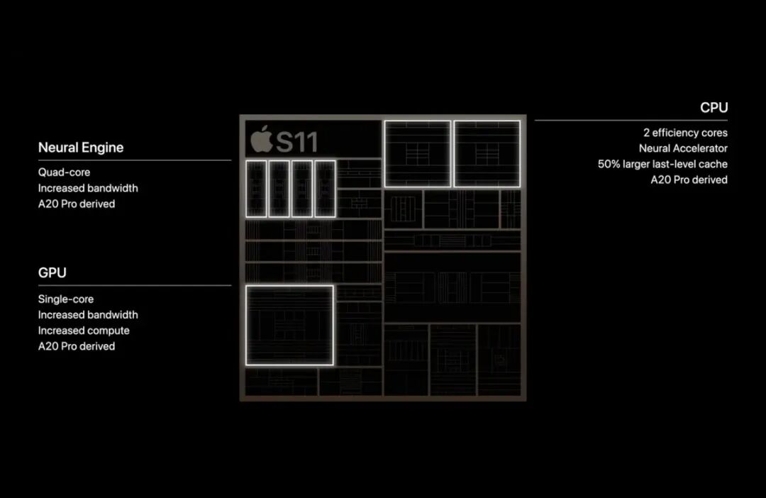
Another new chip from Apple is the S11, which is designed for the Apple Watch Series 12 and Ultra 4. It is equipped with two energy-efficiency cores, a single-core graphics processor and a quad-core AI accelerator.
The brand-new C2 baseband
Apple released the new iPhone 18 Pro models and iPhone Duo today, the company's first foldable iPhone. Both the iPhone 18 Pro and iPhone Duo are equipped with Apple's brand-new custom-designed C2 modem that supports 5G connectivity.
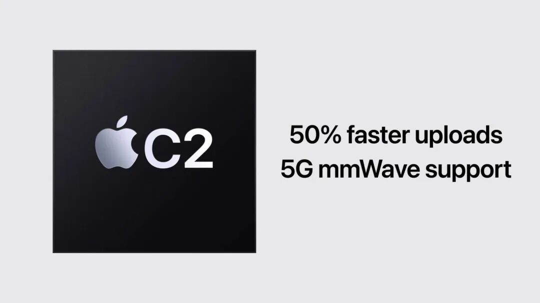
Prior to today's announcement, there were rumors that Apple's self-developed C2 modem would not support millimeter wave 5G networks in the US market, and the company would rely on Qualcomm again to fill this gap for US carriers. But that is clearly not the case, at least as far as millimeter wave support is concerned.
Apple's press release for the iPhone 18 Pro and Pro Max, as well as the technical specifications pages for both models, seem to indicate that the C2 modem is limited to the smaller iPhone 18 Pro model, while the iPhone 18 Pro Max uses a Qualcomm modem. Given that the features of the iPhone 18 Pro and Pro Max are almost identical, the reason for this distinction is unclear.
Apple says the C2 chip uses AI technology to improve the quality and reliability of cellular networks, and now supports millimeter wave technology in the United States. The company claims that compared with the C1X, the C2 also has significantly faster upload speeds while reducing energy consumption by 15%.
As for millimeter wave support, Apple's US specifications list bands n258, n260 and n261, plus 4×4 MIMO sub-6GHz 5G, but the UK specifications only list sub-6GHz.
At the same time, both models are equipped with N1, a wireless network chip designed by Apple that supports Wi-Fi 7, Bluetooth 6 and Thread technologies.
Introduction to the new WMCM packaging
Earlier, we mentioned that Apple has introduced the latest WMCM packaging for its new chip, so what exactly is this technology?
According to introductions, WMCM packaging will adopt MUF (Molded Underfill) technology, which integrates underfill and molding processes.
It is claimed that this packaging technology is an upgraded version of TSMC's InFO-PoP (Integrated Fan-Out Package-on-Package) technology, which integrates advanced packaging technologies such as CoW (Chip on Wafer) and RDL (Redistribution Layer). By horizontally packaging logic chips and DRAM, it replaces the traditional vertical stacking method, achieving significant improvements in heat dissipation and performance. This is also an advanced packaging technology co-developed by TSMC and Apple, designed exclusively for Apple, becoming another major highlight of the A20 processor in addition to its 2nm process.
Industry insiders point out that WMCM can not only achieve thinner packaging, but also integrate more memory, which is critical to meeting the strict requirements for computing power and energy efficiency of future edge AI applications. Chip industry analysts believe that this upgrade is a necessary move to meet the high-performance computing demands in the AI era.
Analysts point out that WMCM is one of the first packaging technologies to blur the boundaries of traditional packaging. It is believed that it may be applied to iPhone packaging in the future, but the logic behind it is very similar to that of High Performance Computing (HPC): shifting from stacked packaging to smarter integration, reducing bottlenecks, improving yield, and preventing heat dissipation from becoming a bottleneck.
WMCM is not a "single technology", but a hybrid mindset.
One of the most illustrative descriptions widely circulated about this technology is that WMCM operates like a hybrid approach that combines the concepts of InFO and CoWoS. This may hint at how TSMC wants the industry to see it:
- InFO showed the world how far fan-out capabilities can go.
- CoWoS taught the world how to scale up integration to improve performance.
- WMCM tries to take the best of both worlds: tighter integration while avoiding the full complexity (and cost) of traditional interposer-intensive approaches.
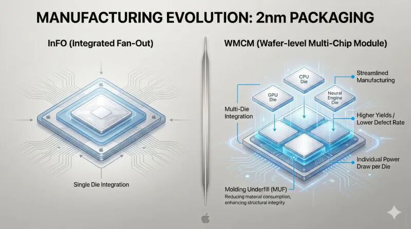
From a packaging perspective, WMCM has multiple structural advantages. By integrating memory directly into the module, it reduces the need for discrete components and eliminates traditional interposers or substrates. The use of molded underfill material further simplifies the stacking structure, reduces material consumption and process steps, and may also free up internal space to accommodate other components, such as a larger battery.
This article is from the WeChat Official Account "Semiconductor Industry Watch" (ID: icbank), written by the Editorial Department, and authorized for release by 36Kr.