Indium Phosphide, a new warning has been issued.
Recently, Jutta Meier, CEO of IQE, stated that access to indium phosphide substrates is becoming a major risk faced by the semiconductor industry due to supply uncertainties brought by export controls. In an interview, Meier pointed out that the core challenge facing the whole industry is "geopolitical restrictions", which refers to the difficulty in obtaining materials for manufacturing high-speed data transmission chips, as supply can hardly meet the demand.
"We are reducing risks through extensive cooperation with different suppliers," Meier noted. "But in the end, if relevant policies are withdrawn, export control licenses will also have an impact on us.
It can be seen from this statement that the already tight supply of indium phosphide has once again sounded the alarm.
What is Indium Phosphide?
To understand why indium phosphide is so important, you first need to know what indium phosphide is.
As one of the three major integrated photonics platforms, indium phosphide (InP) has the longest history. There are good reasons for this: to build light-based electronic circuits, a material that can not only "guide light" but also generate light is required. This means that active components can be manufactured in addition to passive components. As a so-called direct bandgap semiconductor, InP is the only material that can meet both requirements at the same time, while silicon and silicon nitride cannot.
There are many direct bandgap semiconductor materials on the market now, and theoretically all of them can be used to manufacture integrated photonic devices. But from the perspective of practical application, it is completely reasonable for indium phosphide (InP) to become the pioneer of direct bandgap semiconductors.
Looking back at the development history of indium phosphide, it can be traced back to the invention of the first semiconductor laser in 1969. Later, a photonic integrated circuit composed of a laser and a modulator came out in 1987. This circuit was partially based on indium phosphide (InP) material. Since then, the number of components integrated on a single InP chip has grown exponentially, similar to Moore's Law in the electronics field. Today, photonic integrated circuits (PICs) with more than a thousand integrated components can already be fabricated in research environments.
Although InP can be applied in many scenarios, its most prominent application field is undoubtedly optoelectronics. InP lasers provide light sources for optical communication systems around the world, covering optical fiber connections, networks, free-space optical communications and other aspects. Streaming media companies, mobile communication operators and smartphone manufacturers are all inseparable from InP. Specifically, in the field of communication technology, it is only a matter of time before InP photonic integrated circuits (PICs) are applied to data centers, fiber-to-the-home (FTTH, namely fiber-to-the-x, referring to homes or other types of buildings), 5G base station connections and many other fields. After all, with the growing global demand for bandwidth, the advantages of indium phosphide chips cannot be ignored.
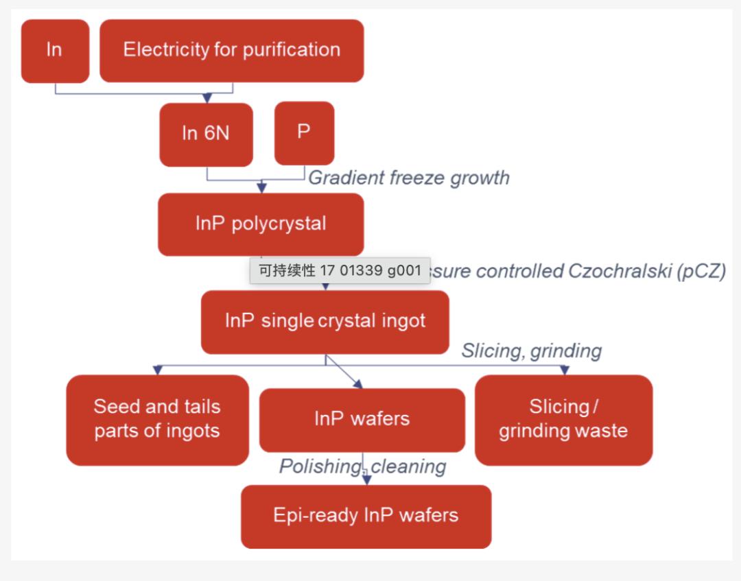
As shown in the figure above, the fabrication of indium phosphide (InP) wafers starts from two basic raw materials: high-purity indium and phosphorus. First, indium purified to 6N level and phosphorus are placed at both ends of a quartz container respectively, and heated under high pressure: indium is melted above 1062℃, while phosphorus is maintained at about 560℃ to form vapor, the two react to generate liquid indium phosphide, which is then slowly cooled to obtain polycrystalline material. Next, the polycrystal is melted again, and the controlled pressure Czochralski method (pCZ) is used to grow the single crystal ingot. Through precise control of the temperature gradient, phosphorus vapor pressure and boron oxide liquid encapsulation, phosphorus volatilization is suppressed and low-defect single crystal is obtained. At the same time, elements such as iron, tin and zinc can be added according to requirements to achieve different electrical properties. Finally, the single crystal ingot goes through processes such as crystal orientation positioning, outer circle grinding, diamond slicing, double-sided polishing and chemical cleaning, to produce indium phosphide wafers with flat surface and extremely high cleanliness, which provide basic materials for the epitaxial fabrication of optical communications, silicon photonics and high-speed optical chips.
It can be seen that every link may become a bottleneck restricting the supply of indium phosphide. But this round of demand surge starts with data centers.
Data Centers, Driving Explosive Demand
First of all, we must reiterate that indium phosphide itself is not an end product, but a III-V compound semiconductor material, which is mainly used to manufacture optoelectronic devices such as lasers, detectors and modulators for optical communications. Among them, distributed feedback lasers (DFB Laser) and continuous wave lasers (CW Laser) are the main products made of indium phosphide, and they are also the most important components of optical modules. What really triggered this round of demand for indium phosphide is not consumer electronics, but data centers.
As the scale of AI training and reasoning continues to expand, hundreds of thousands of GPUs need to form ultra-large-scale clusters through high-speed optical interconnection. Optical modules are moving from the 400G and 800G era to the 1.6T and even 3.2T era. Compared with VCSEL, indium phosphide lasers can provide higher power, longer transmission distance and multi-wavelength capability, becoming the core light source of silicon optical modules, and making indium phosphide, which was previously a relatively niche material, rise to become one of the most scarce key materials in AI infrastructure.
It needs to be emphasized that every speed upgrade of optical modules will not only double the bandwidth, but also increase the complexity:
- 800G transceivers usually use four optical channels.
- 1.6T modules use eight channels
- Each channel requires its own laser and detector — which is usually based on indium phosphide (InP).
Therefore, when the industry transitions from 800G to 1.6T, the amount of InP used per module almost doubles.
Now, we turn to modern AI architectures. The design of these platforms is inspired by NVIDIA. Their design goal is to achieve terabit-level bandwidth per rack. This means that each rack requires hundreds of optical modules, each deployment requires thousands of racks, and each hyperscale data center requires millions of indium phosphide laser components every year.
We can see the growth of these demands more intuitively from Yole's data forecast.
Yole states that AI clusters need a 70-fold increase in the number of interconnections every two years. Channel speed only doubles every four years, switch bandwidth doubles every two years, and the number of AI parameters doubles every four months. This "interconnection barrier" makes the transition to 1.6T, 3.2T and CPO crucial for every supplier, rather than just a gradual upgrade.
Yole estimates that the optical module market size will grow from about 10 billion US dollars in 2021 to 112 billion US dollars by 2031 (with a compound annual growth rate of about 35%), which is mainly driven by the fact that hyperscale data centers are expected to reach 670 billion US dollars in capital expenditure in 2026 alone, and a total capital expenditure of 5.3 trillion US dollars from 2026 to 2031.

The demand for indium phosphide behind this surge is imaginable. However, we must also realize that the InP supply chain was not originally designed to meet the demands of AI scale: the production of InP substrates is controlled by a very small number of suppliers, epitaxial wafer growth is more concentrated, and the production of high-speed externally modulated lasers (EML) is mainly dominated by two companies.
This high concentration brings both industrial risks and geopolitical risks. A considerable part of InP substrate production is related to China, while advanced epitaxy technology is highly concentrated in Taiwan region. When China implements an export license system for indium-related materials, delays spread across the entire system almost immediately.
Lumentum, a major optical communication manufacturer that makes related optical chips, warned in August that the demand for indium phosphide lasers in AI data centers has multiplied, and the supply shortage may be more severe than that of memory. Even after Coherent doubled its indium phosphide production capacity, it still cannot meet the market demand.
That is precisely why the industry is paying close attention to this material.
Self-Rescue After the "Supply Bottleneck"
After encountering the above problems, the industry has started to take self-rescue measures. Apart from the upstream material supply, substrates are one of the key links.
Substrates can be understood as the "foundation" of optical chips. Whether it is CW lasers and EML lasers used in data centers, or high-speed modulators and photodetectors, they must first undergo epitaxial growth on a high-quality indium phosphide single crystal substrate. The defect density, crystal uniformity and flatness of the substrate directly determine the yield, service life and transmission performance of the devices. Therefore, it is widely recognized in the industry that whoever masters high-end InP substrates holds the most irreplaceable link in the AI optical interconnection industrial chain.
In this link, Japan's Sumitomo Electric is almost an unavoidable name. Sumitomo has been deeply involved in indium phosphide materials for decades, and is the world's largest supplier of InP substrates. It has long occupied about 40% of the high-end semi-insulating substrate market, and is also an important source of materials for the AI optical module ecosystem such as NVIDIA and Broadcom. Its core advantage does not lie in equipment, but in the Liquid Encapsulated Czochralski (LEC) crystal growth process — through precise control of the temperature field, phosphorus vapor pressure and liquid encapsulation environment, it can continuously produce 6-inch indium phosphide wafers with low dislocation and high uniformity. This process relies heavily on long-term experience accumulation. Even with the same equipment, it is difficult to replicate it in a short time, so Sumitomo has become one of the most representative "bottleneck-forming" enterprises in the global indium phosphide supply chain.
If Sumitomo Electric represents high-end semi-insulating substrates, then JX Advanced Metals from Japan represents a vertically integrated indium phosphide material system.
JX is one of the few enterprises in the world that has the capabilities of high-purity metal purification, indium phosphide single crystal growth and substrate processing at the same time, with more than 40 years of InP substrate manufacturing experience. Its products are mainly used in data center optical modules, lasers, photodetectors and high-speed electronic devices, and are famous for low dislocation density, high flatness and stable epitaxial consistency. It is an important material supplier in the global AI optical communication industry chain.
AXT (Beijing Tongmei) is one of the most critical enterprises in the global indium phosphide substrate field, and also the only Sino-US background manufacturer that has entered the global first tier.
AXT is headquartered in Silicon Valley, USA, and the actual indium phosphide manufacturing entity is its wholly-owned subsidiary, Beijing Tongmei. The company focuses on indium phosphide (InP), gallium arsenide (GaAs) and germanium (Ge) substrates. It is one of the few enterprises in the world that can stably mass-produce 2–6 inch InP single crystal substrates. Its products are widely supplied to optical chip and epitaxial manufacturers such as IQE, LandMark, VPEC and Coherent, and it is also an important upstream material source for AI data center optical modules.
Different from the LEC route adopted by Sumitomo and JX, AXT's core competitiveness comes from its self-developed VGF (Vertical Gradient Freeze) crystal growth technology. VGF can obtain a more uniform temperature field and lower thermal stress, and has advantages in the growth of large-size indium phosphide crystals. Therefore, Beijing Tongmei has long been regarded as one of the representative manufacturers of 6-inch InP substrates.
From the data point of view, the three major substrate manufacturers above have locked most of the indium phosphide substrate demand. Facing this round of explosive growth, they are also expanding their production capacity.
In July this year, it was reported that Sumitomo Electric of Japan expanded its indium phosphide substrate production capacity to 3.1 times to meet the rapid demand of AI; JX Metals plans to invest 120 billion yen to expand its InP substrate production capacity by 7-10 times; AXT plans to double its indium phosphide production capacity by the end of 2026 based on the level of Q4 2025, and double it again in 2027. The company is also advancing from mass production of 3-inch and 4-inch InP substrates to 6-inch substrates.
All in all, all parties are making their own efforts to meet the demand of the industrial chain.
Closing Remarks
In the author's opinion, in the next five to ten years, indium phosphide will not exit the stage. On the contrary, it will become one of the most strategically valuable materials in the era of AI optical interconnection. But its development direction will no longer be independent competition, but form a new pattern of "division of labor and cooperation" with silicon photonics and thin-film lithium niobate.
Silicon photonics is responsible for large-scale integration, realizing low-cost and high-density optoelectronic integration with CMOS process; thin-film lithium niobate, with higher bandwidth and lower power consumption, has become an important choice for next-generation high-speed modulators; while indium phosphide continues to firmly occupy the core position of lasers and light sources, especially in high-speed optical communications in the 1310nm and 1550nm bands, there is almost no mature material that can completely replace it in the short term.
The real focus of competition will also shift from a single material to heterogeneous integration. The future optical chip is very likely to be a combination of "silicon base + indium phosphide light source + lithium niobate modulation", which integrates different materials into the same device through advanced packaging, to achieve the best balance between performance and cost.
In a recent sharing session, Lumentum shared its indium phosphide technology roadmap layout, which can be summarized into three directions: higher speed, higher power, and more wavelengths.
Over the past ten years, Lumentum has continuously advanced InP EML (Electro-absorption Modulated Laser) technology, evolving from 40Gbps to 400Gbps per channel, and further upgraded to a differential architecture, which has been introduced into actual optical transceiver platforms to provide core light sources for 800G and 1.6T optical modules.
At the same time, the company is expanding indium phosphide to ultra-high power lasers. For CPO, higher output power of a single laser means that the number of lasers can be reduced, the complexity of the optical engine can be lowered, and the overall system cost can be improved. Therefore, high-power InP lasers are regarded as one of the key technologies for future CPO.
In terms of bandwidth expansion, Lumentum chose the "Wide and Slow" route, which is to expand the total bandwidth by increasing the number of DWDM wavelengths, rather than simply increasing the single baud rate. Its latest demonstrated 16-wavelength InP light source has high optical power of about 350mW, narrow linewidth and low noise characteristics, providing a new evolution direction for ultra-high-speed optical interconnection of next-generation AI data centers.
Based on the above discussion, we believe that for the industry, the biggest challenge for indium phosphide is not being replaced, but whether it can keep up with the capacity and cost requirements of AI; and the biggest opportunity is that with the full popularization of 800G, 1.6T and even higher-speed optical interconnection, it will become the most scarce and indispensable strategic material in the entire data center optical network.
This article is from the WeChat Official Account "