HBM is undergoing major changes
The competition in the HBM market is quietly shifting to a new battlefield. Over the past few years, market discussions around HBM have almost exclusively focused on SK Hynix, Samsung, and Micron: who has the more advanced DRAM process, who can stack up to 12 or 16 layers, who delivers higher TSV and packaging yield, and who can eventually secure a spot in NVIDIA's supply chain.
However, with the advent of HBM4 and HBM4E, a group of previously under-the-radar new players are emerging in this industry — wafer foundries.
Recently, according to reports from South Korean media and DIGITIMES, SK Hynix is considering introducing Intel Foundry into the HBM4E supply chain as a second foundry source for HBM Base Die, to reduce its reliance on TSMC and improve supply resilience. Regardless of whether Intel can eventually win the order, the underlying industrial shift has already been very clear: starting from HBM4, an HBM product is increasingly inseparable from advanced logic processes.
The real game-changer is the previously overlooked chip at the very bottom of HBM — the Base Die.
HBM is becoming less and less like traditional memory
To understand why HBM is turning into a wafer foundry business, we must first look at HBM4, the key technical watershed.
In HBM3E and earlier technology generations, the structure of HBM was relatively straightforward: the upper layer is a multi-layer DRAM stack (Core Die), and the bottom layer is a single Base Die. In the past, this Base Die was mainly responsible for physical support, TSV (Through-Silicon Via) routing, and basic signal routing. Thanks to its simple functions, the three major memory vendors (SK Hynix, Samsung, Micron) could easily produce it using their own 10nm-class DRAM processes.
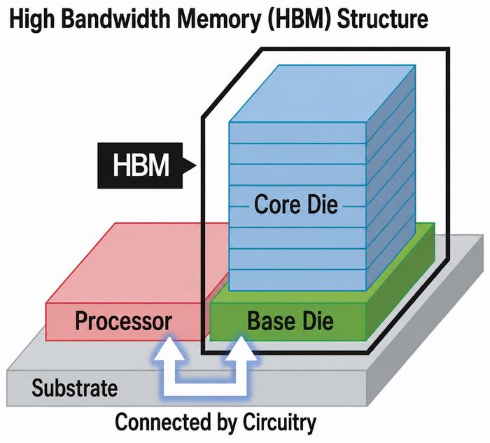
But several important changes have taken place in HBM4.
On one hand, the interface density has doubled physically. The bus interface width of HBM4 has directly doubled from 1024-bit to 2048-bit. On this basis, NVIDIA has further increased the per-pin rate to over 11Gbps on the Rubin platform. To fit the doubled TSV and PHY (physical layer) circuits into an extremely tiny chip area, the wiring density and metal layer count of traditional DRAM nodes have hit their physical limits.
On the other hand, logic functions are deeply embedded. In pursuit of ultimate energy efficiency and ultra-low latency, GPU and ASIC vendors are starting to require that memory controllers, DFT (Design for Test) circuits, and even computing modules for specific algorithms be directly integrated into the Base Die.
SK Hynix also noted on its official website that "in HBM4, the role of logic chips is becoming increasingly prominent. The R&D direction of HBM4 is to improve the performance of the base chip, enhance the connectivity between the HBM stack and the logic chip, and reduce power consumption at the same time."
The Base Die has evolved from a relatively simple chip to a complex Logic Base Die. This hits the process barrier of original memory manufacturers: the fabs of memory manufacturers are basically not equipped with 12nm, 5nm or even more advanced process lines for producing high-performance logic chips, and the two follow completely different manufacturing logic. Because DRAM manufacturing pursues memory cell density and cost, while complex logic circuits require logic transistor performance, wiring density, and advanced EDA design capabilities.
When more and more logic is integrated into this "memory", the business that once belonged exclusively to memory vendors is quietly turning into a wafer foundry business. As a result, wafer foundries are starting to step onto the stage.
In 2024, SK Hynix and TSMC announced a partnership to co-develop HBM4. The statement released by the two parties at that time was already very thought-provoking — they aimed to establish a tripartite cooperation model consisting of IC design companies, wafer foundries and memory vendors. The first target of their cooperation is the Base Die.
Before HBM3E, SK Hynix basically produced its own Base Die; starting from HBM4, it introduced TSMC's advanced logic processes. This has actually changed the HBM industry division of labor that has lasted for many years. Previously, the main components of an HBM product were DRAM manufacturing + TSV + 3D stacking packaging. Now it is increasingly approaching the structure of: DRAM Core Die + Logic Base Die + Foundry + TSV + Advanced Packaging.
HBM, which used to be a "special type of memory", is increasingly becoming a small Chiplet system.
The era of customized HBM is accelerating
With the increasing logic complexity of Base Die, HBM is moving from standard parts in the past to customized products.
At this year's TSMC Technology Symposium, SK Hynix revealed that in the future, by adopting Base Die manufactured with TSMC's advanced logic processes, HBM will be further pushed from standardized products to Custom HBM, and the integration of Memory and Logic will be strengthened. Meanwhile, in Silicon Valley, SK Hynix has been reported to be setting up a dedicated HBM architecture design team, whose recruitment positions not only cover traditional DRAM expertise, but also require mandatory experience in digital design, PDN (Power Distribution Network) and sub-3nm advanced foundry processes.
This is far from the working mode of a traditional memory company, and is becoming more and more similar to that of an ASIC company.
In SK Hynix's product roadmap after HBM4, HBM4E and customized HBM are listed as key development directions. SK Hynix's iHBM solution is a thermal management technology for next-generation HBM products, designed to improve its operational stability and efficiency in high-density, high-bandwidth scenarios.
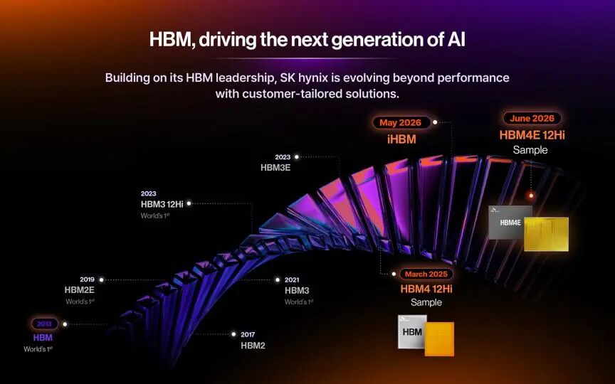
(Image source: SK Hynix)
The core force driving this transformation comes from the downstream AI chip giants' desire to "break the memory wall".
The so-called Custom HBM, in essence, has begun to evolve from "customized memory" to Memory-Compute Co-design. This has also changed the most critical relationship in the HBM industry. In the past, memory vendors mainly produced standard products. Samsung, SK Hynix, and Micron developed DDR, LPDDR or HBM according to JEDEC standards, and then sold them to customers.
But AI chips are completely different. NVIDIA, AMD, Google, Amazon, Microsoft, and a growing number of cloud vendors that develop their own ASICs have different requirements for Memory Bandwidth, power consumption, interfaces, and packaging area. Standardized HBM is increasingly unable to meet the needs of all customers. Therefore, HBM is moving closer to a business model that is very familiar to the ASIC industry: joint specification definition — co-design — foundry tapeout — advanced packaging — customer verification.
The player that pushed this trend to a climax is NVIDIA. On August 26, NVIDIA announced a new technology called NVHBM. In traditional AI hardware architectures, the memory controller usually occupies extremely valuable advanced process area inside the GPU or XPU computing core. In NVHBM, NVIDIA directly implemented a bold redesign: the memory controller is removed from the GPU and directly embedded into the HBM's Base Die.
According to data released by NVIDIA, compared with standard HBM4E, NVHBM can deliver up to 30% higher memory bandwidth and 15% lower power consumption, while freeing up up to 25% more XPU computing core area. Annapurna Labs under Amazon has become one of the first chip design teams to participate in the R&D of this architecture.
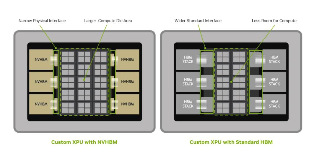
Comparison of chip area savings between NVHBM and standard HBM
(Image source: NVIDIA)
This is far more than an ordinary HBM specification upgrade. Because the previously clear boundary between HBM and GPU is blurring. In the past, the GPU was responsible for computing and HBM for storage. In the future, it may become: GPU + Logic Base Die + DRAM jointly form the computing system. The migration of the Memory Controller is just the first step. Theoretically, more logic related to data movement, address mapping, cache management, and even specific computing tasks may be migrated to the Base Die in the future.
Three major HBM vendors, three different foundry strategies
At present, Samsung, SK Hynix, and Micron have actually embarked on three different development paths.
SK Hynix has chosen the most typical specialized division of labor model. It is responsible for DRAM Core Die and HBM technology itself, and entrusts the manufacturing of advanced Logic Base Die to foundries such as TSMC. According to recent reports from South Korean media cited by TrendForce, the Base Die used in SK Hynix's mass-produced HBM4 is manufactured with TSMC's 12nm-class process; and for future HBM4E, as logic complexity further increases, the industry is already discussing migration to more advanced nodes.
At the same time, due to the rapid increase in the cost of advanced logic Base Die, SK Hynix has also been reported to be considering Intel Foundry as a potential second supply source.
Samsung has taken the opposite approach. Samsung has both memory and foundry businesses, so from the very beginning it has chosen a more thorough vertical integration route. The HBM4 mass-produced by Samsung this year uses 1c DRAM Core Die, while the Base Die is directly manufactured using its own foundry's 4nm logic process. HBM4E also continues the 1c DRAM + 4nm Logic Base Die combination. Samsung has even planned to push the Base Die to 2nm process in subsequent HBM products.
In the past, Samsung's simultaneous operation of memory and foundry businesses was often considered overly complex, but in the Custom HBM era, this model may generate new synergy advantages. Because Samsung can theoretically complete all the DRAM, Logic, and advanced packaging required for an HBM product internally.
The third path comes from Micron, which is also shifting from independent development to embracing foundry partners. In the early stage of HBM4, Micron still emphasized in-house development and manufacturing of CMOS Logic Base Die, but for HBM4E, its strategy has changed significantly. Micron explicitly stated in its investor materials that both the standard and customized versions of the Logic Base Die for HBM4E will be produced in cooperation with TSMC, and the company expects that the gross margin of HBM4E using Customized Base Logic Die will be higher than that of standard products.
This point is critical. Because it shows that HBM vendors themselves have begun to admit: one of the biggest added values of HBM in the future may no longer only come from DRAM, but from the customized logic in the Base Die.
For wafer foundries, the HBM transformation means huge new growth opportunities.
In the past AI server industrial chain, foundries (represented by TSMC) have firmly occupied two highest-value sectors: GPU/ASIC logic chip foundry + CoWoS advanced packaging. Now, a third high-value sector is taking shape — the HBM logic Base Die.
Of course, compared with GPUs, the wafer demand scale for HBM Base Die is not at the same level. But its importance lies in: every additional HBM product means an additional Logic Die. High-end AI accelerators usually carry 6 to 8 HBM units per chip, and with the migration of Base Die to 12nm, 5nm or even more advanced nodes in the HBM4/4E era, the value share of wafer foundries in the entire AI memory system will expand exponentially.
As HBM evolves from HBM4 to HBM4E and Custom HBM, the Base Die process becomes more advanced, the area becomes larger, and the logic becomes more complex, the value of the foundry in each HBM unit will also increase accordingly.
This is why Intel may have the opportunity to re-enter this competition. If Intel Foundry directly fights for the main Compute Die orders of top GPUs from NVIDIA, AMD and other vendors, the difficulty is extremely high. But HBM Base Die may be a completely different entry point. It requires advanced logic manufacturing capabilities, but does not bear the risk of being the entire system's computing core like a GPU; at the same time, memory vendors such as SK Hynix have the motivation to reduce supply concentration and cost.
For Intel, this may be a more realistic incremental market than directly challenging TSMC's advanced GPU foundry business.
Closing remarks
Over the past few decades, the most typical business model of the memory industry has been standardization. The more standardized the product, the larger the scale, and the lower the cost. Whether it is DRAM or NAND, most of the competition between vendors revolves around process, capacity, yield and cost. However, AI is breaking this logic. HBM4 brings Logic Base Die into advanced processes, HBM4E continues to increase the complexity of Base Die, and NVHBM further embeds the Memory Controller directly into HBM. Moving forward along this path, HBM will likely become more and more difficult to be simply defined as "memory". It will gradually evolve into a Memory System composed of DRAM, Logic, interconnection and advanced packaging.
As a result, the competition in the HBM industry is also changing. In the past, it was SK Hynix vs Samsung vs Micron, but in the future it will more likely become a portfolio competition between memory vendors + foundries + AI chip vendors + advanced packaging service providers. What seems to be just SK Hynix considering placing a Base Die order with Intel Foundry is far more significant than a single foundry order. It means that the boundary of wafer foundries has pushed one step further into the AI system.
After CPU, GPU and ASIC, the next chip to enter the advanced logic foundry system may be the HBM Base Die, which has long been regarded as part of memory. HBM is still a type of memory, but starting from HBM4, it has become more and more like a complete chip system.
In the second half of the HBM industry, the competition hotspot will not lie in DRAM itself, but in the Base Die that sits at the very bottom.
*Disclaimer: This article is the original work of the author. The content of the article represents the author's personal views only. The reprint by Semi-Industry Observer is solely to convey a different perspective and does not represent Semi-Industry Observer's endorsement or support for the views expressed. If you have any objections, please contact Semi-Industry Observer.
END
This article is from the WeChat official account "Semi-Industry Observer" (ID: icbank), author: Du Qin DQ, published with authorization from 36Kr.