Waymo's self-developed chip is exposed: 1000 TOPS is only on the surface, and the 160 TOPS performance is what really matters.
A chip is officially advertised to have a computing power of over 1000 TOPS, but the actual published dense computing throughput is only 160 TOPS.
Is Waymo "inflating the figures", or is the 1000 TOPS figure itself not that important?
The answer is likely the latter.
The most noteworthy part of Waymo's self-developed chip this time is not how many TOPS of computing power it has, but Waymo has shifted the competition of autonomous driving chips from "piling up computing power" to "competing for data handling efficiency".
01
1000 TOPS,
Why is the actual value only 160 TOPS?
On August 20, Waymo officially announced the launch of its self-developed 5-nanometer chip, and detailed this self-developed chip at the Hot Chips conference on August 24.
On Waymo's official website, Waymo claims that its computing power exceeds 1000 TOPS.
For ordinary people, the computing power value is the TOPS value, the higher the better, and Waymo is no exception.
But at the Hot Chips conference, in front of a professional audience, there is no need for Waymo to only emphasize the peak computing power value.
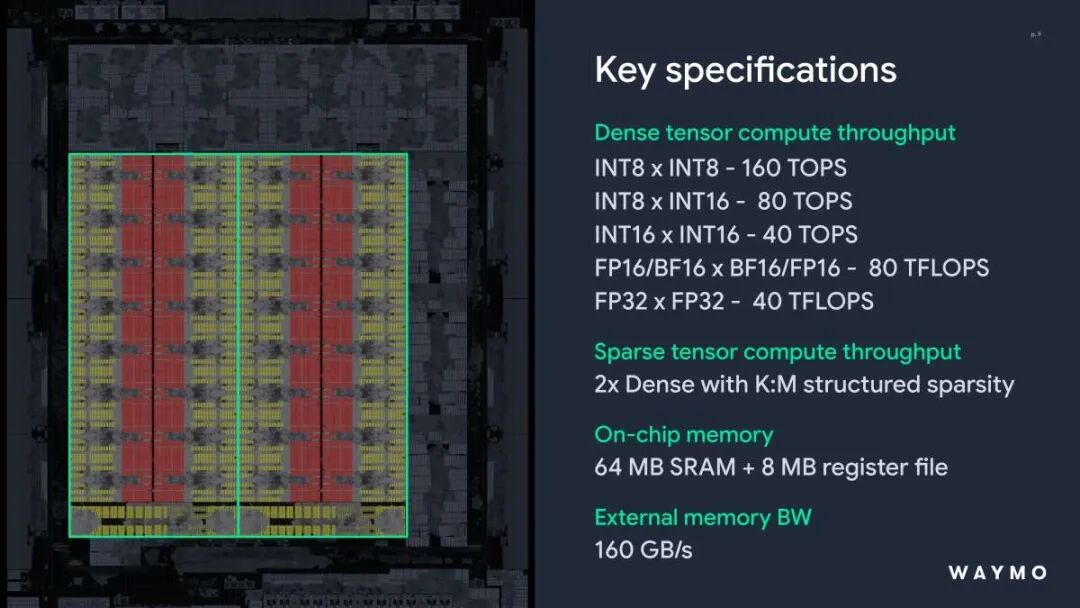
The dense tensor computing throughput of this chip is only 160 TOPS. Like NVIDIA, Waymo has also achieved 2x structured sparsity, which means the throughput under sparse mode is 320 TOPS.
Does this mean that Waymo's computing power is not high?
Not exactly, its actual computing power should be much stronger than many chips that claim to exceed 1000 TOPS.
The industry usually publishes theoretical peak computing power, and there is often a clear gap between the theoretical TOPS and the real model throughput and latency.
This time, Waymo clearly specifies the throughput capacity under dense/sparse and different precisions, which makes the 160 TOPS figure more reference-worthy.
For example, TOPS is more like the "theoretical maximum speed" of a car.
But when it is actually running, what determines whether a car is fast or not is not only the maximum speed, but also factors such as road conditions, gearboxes, tires, and power systems, to see if the power can be truly released.
The same goes for chips. 1000 TOPS is the theoretical peak, which does not mean that the actual model can continuously run at 1000 TOPS.
The TOPS of a chip is like the horsepower of a car: the figure on paper is important, but what really determines the experience is "how much power can be actually utilized".
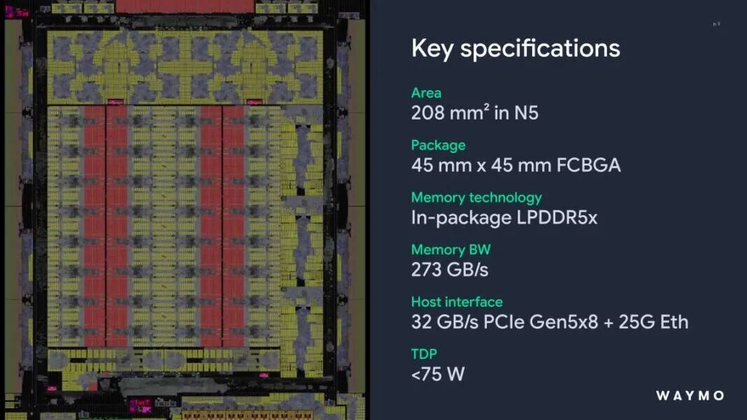
Waymo's this chip has an area of 208 square millimeters, which is about half of the Li Auto Ma 100. It adopts TSMC's 5-nanometer process, integrated MOP memory and packaging design, and the host interface uses the most advanced 8-Lane PCIe 5.0 with a bandwidth of 32GB/s, which is 25 times that of 10 Gigabit Ethernet. It is also equipped with 25G Ethernet, and the power consumption of the entire chip is less than 75W.
This power consumption level is very friendly to the vehicle heat dissipation environment.
02
Why is Waymo no longer satisfied with buying off-the-shelf chips
Many people may be curious about one question: Waymo already has a mature Intel computing system, so why does it still develop chips on its own?
In fact, Waymo has considered self-developed chips since 2016, but the models are changing so fast that the chip design has to be iterated again and again.
For a Robotaxi company like Waymo, the coupling between models, algorithms, data and hardware is getting deeper and deeper, and there is a lot of waste of unused resources on general-purpose chips.
Self-developed chips are not just for cost reduction, their significance can be divided into three layers:
Design chips for your own models. It is not "can run any AI model", but "design whatever my model needs".
Reduce data handling. The real process of computing is "compute → move data → compute again → move data again". If a lot of time is spent on data handling, no matter how many computing units there are, it will be meaningless.
Hardware and software co-design. Designing models, compilers and chips together is what makes Waymo's chip really worthy of attention by the automotive industry.
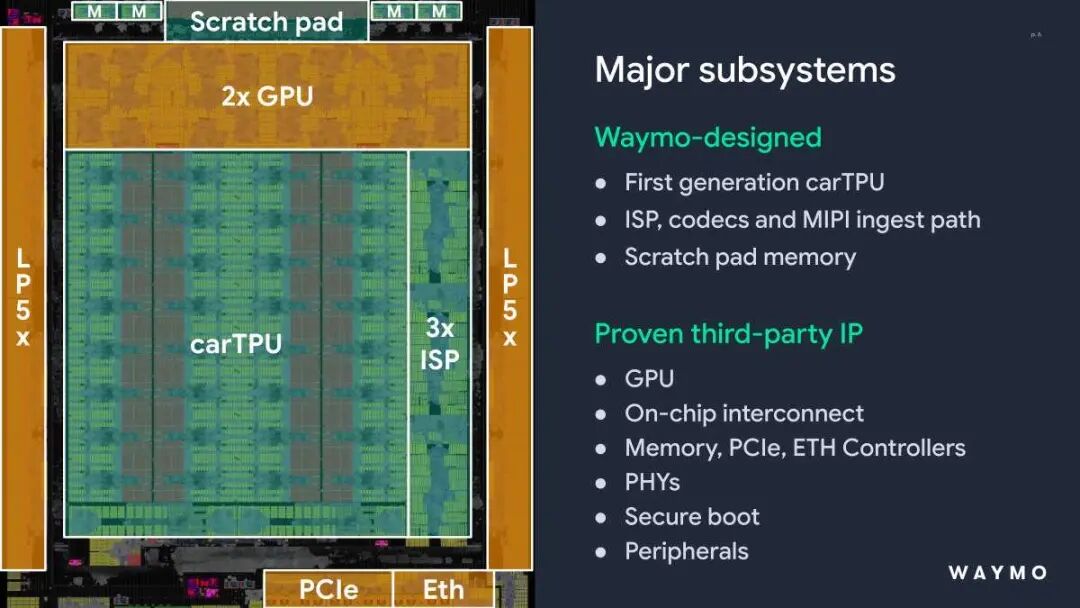
The core of Waymo's chip architecture is carTPU. The IPs purchased by Waymo include GPU, on-chip interconnect, LPDDR5X controller and PHY, PCIe controller and PHY, Ethernet controller and PHY, security root, etc. It has self-developed video ISP, codec, MIPI and scratchpad registers.
It should be noted that this does not affect the authenticity of "self-development".
Today's "self-developed chips" are no longer fully manufactured from transistors on their own, but around their own models and workloads, re-design the key computing paths: chip architecture, data flow, video processing, compilers and computing cores.
That's exactly what Waymo did.
Pieter Kapsenberg, the core figure of Waymo's self-developed chips, joined Intel in 2005, joined Google's video codec hardware department in 2014, and joined Waymo in 2016.
Another core figure, Sabareesh Ravikumar, who previously worked on design at Apple, joined Waymo in September 2017, and is especially good at storage system design.
03
What Waymo really wants to solve
is not computing power, but "data cannot be moved efficiently"
In fact, in the Transformer era, basically after exceeding 100 TOPS, the marginal value of the TOPS figure drops sharply, and the bottleneck is completely in the storage part.
About 70-90% of the time, the computing units are idling while waiting for the storage system to move data, which is the well-known Roofline model. The automotive industry cannot use multiple batches, and the batch is generally 1, which makes this phenomenon more obvious.
Now we are entering the era of world models, that is, the DiT (Diffusion Transformer) era, and the storage bottleneck is even more prominent.
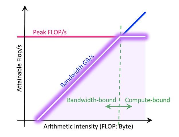
Roofline Performance Model, the X-axis of the Roofline model curve represents Flops/byte (GFlops per byte), i.e. operation intensity, and the Y-axis represents GFlops/s (GFlops per second)
This is the reality revealed by the well-known Roofline model in the field of chip design: there are two limits for chips, one is insufficient computing power, and the other is that data cannot be fed fast enough. Its core is only one formula: Actual performance = min (peak computing performance, memory bandwidth × arithmetic intensity).
The horizontal line represents the peak floating-point performance of the computer or chip, and the actual performance of any floating-point operation will not exceed this line, because it represents the hardware limit.
The slanted line represents the maximum floating-point operation performance supported by the computer's memory system under different operation intensities.
And Waymo believes that many AI tasks today are not really encountering the former situation, but the latter. In most scenarios at present, the arithmetic intensity of operators is lower than the equilibrium point of the chip, and the performance is limited by memory bandwidth.
In other words, the computing speed is very fast, but the data handling cannot keep up.
AI models have both "large-batch computing" scenarios (matrix multiplication, i.e. GEMM) and scenarios of "calculating one data at a time" (matrix-vector multiplication, i.e. GEMV).
The latter GEMV calculation is particularly sensitive to memory bandwidth and data handling efficiency.
This is exactly the most common computing mode for real-time reasoning in autonomous driving.
Waymo's this chip is obviously optimized for this type of calculation.
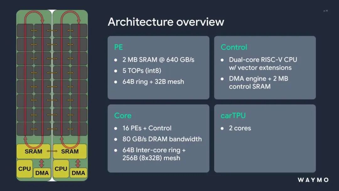
After understanding this, looking at Waymo's architectural design, there is a causal relationship behind each parameter, rather than a simple list of parameters.
Among them, the three most critical designs are:
5nm advanced process, which proves that Waymo is not just making an auxiliary chip, but has truly entered the first echelon of high-performance AI chip design;
Large-capacity, high-bandwidth on-chip SRAM. Each carTPU contains two cores, each core contains 16 computing units (PEs), each core includes 2MB of SRAM with a bandwidth of up to 640GB/s. The total on-chip SRAM of the entire chip reaches 64MB, plus 8MB of register files. This directly serves the core goal of "data handling is more important than pure computing power", keeping data on the chip as much as possible and avoiding unnecessary trips to external memory;
GEMV + dual DMA architecture. In Waymo's PE architecture, each PE contains 4 computing slices, which can complete 512 INT8 GEMV operations per cycle. Waymo is obviously a chip specially designed for GEMV operators. DMA refers to Direct Memory Access. There is Mesh DMA between PEs, and Ring DMA for weights and calculation value output. The two sets of DMA work in division of labor to minimize data handling. This directly proves that this chip is customized around Waymo's own autonomous driving workload.
In addition, the flexible GEMV path can be adapted to different computing primitives (referring to the most basic, indecomposable basic operations, data types or elements).
Waymo will dynamically adjust the operation mode to achieve maximum PE utilization.
This is crucial because it ensures that the Tensor Cores always maintain high load operation when processing various network layers with very different forms.
04
Autonomous driving chips
are entering the era of integrated hardware and software
Hardware is only half the story, and software is the real difficulty of this chip.
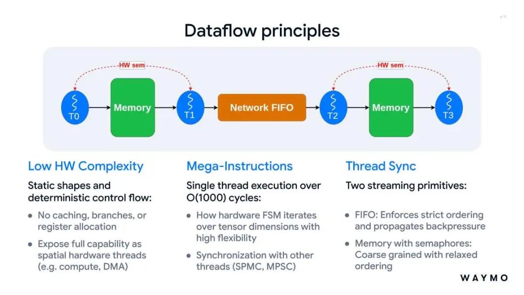
Waymo's data flow principle ensures the streamlining of hardware.
Waymo uses deterministic "mega-instructions" with static shapes, which are executed in a single thread for about a thousand clock cycles without involving cache or branch operations.
At the same time, FIFO queues and semaphore-based storage mechanisms are used to coordinate the data order and backpressure control between computing threads and DMA threads.
This means that the difficulty of its compiler design is extremely high.
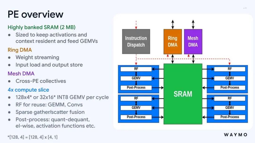
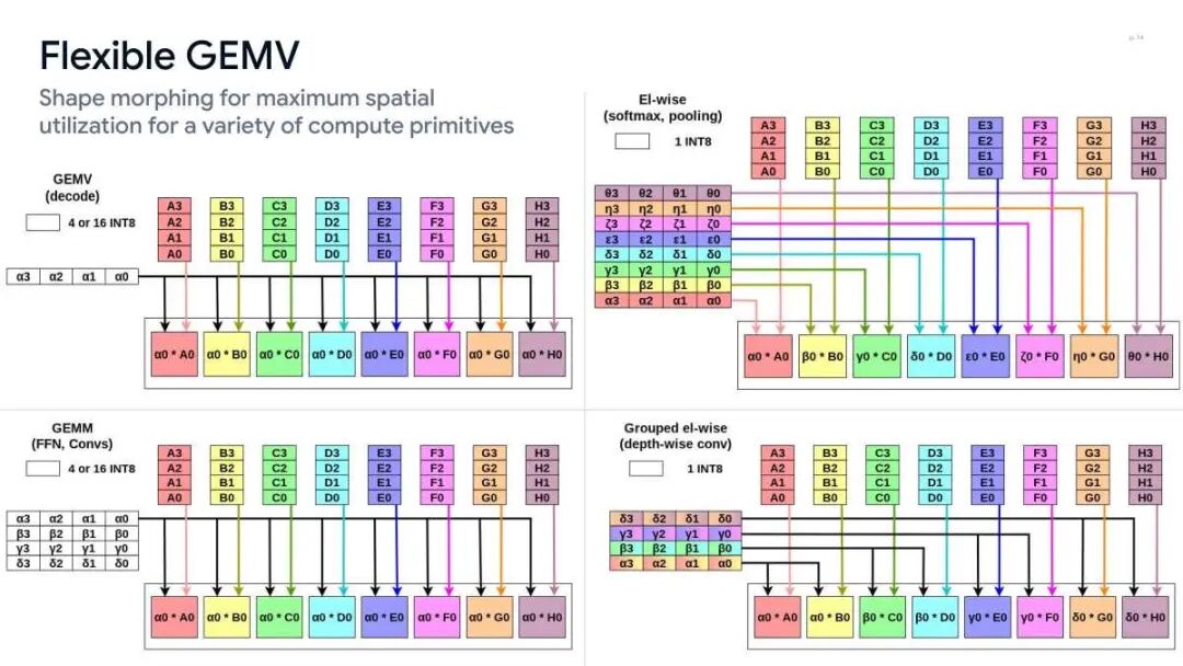
Path of Waymo PE when processing different operators
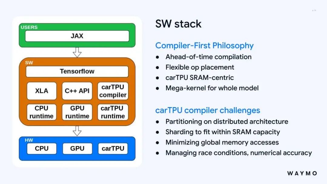
Waymo's software architecture follows the design concept of "compiler first":
It adopts the ahead-of-time (AOT) compilation method to build a super-large mega-kernel for the entire model, and splits it to fit the SRAM. The compiler is responsible for managing partitions, global memory data transmission, race conditions and numerical precision.
The upper layer is connected to Google's mainstream frameworks such as JAX and TensorFlow. Developers can write models in a familiar way, and leave the rest to the compiler.
This is essentially: designing models, compilers and chips together.
Waymo emphasized at Hot Chips that the actual achieved performance is more important than the ideal TOPS figure.