NVIDIA has an insatiable demand for diamonds, and the development of AI is inseparable from Henan's "lab-grown diamonds".
In January this year, Jensen Huang, CEO of NVIDIA, met a Henan-based diamond entrepreneur in Beijing.
One is the person best at "selling shovels" in the AI era, and the other is a leading figure in Henan's lab-grown diamond industry. The conversation between the two behind closed doors sounded rather surreal.

After all, the most widely known story of Henan's lab-grown diamond industry in previous years is that it drove the price of diamonds down to the level of cabbage, completely disrupting the entire pricing system of cultured diamonds.
We have previously made a dedicated analysis of this industrial chain (click here to review). No one back then could have imagined that these Henan factories that kept driving diamond prices lower would one day be targeted by AI chip giants.
01
AI chips are overheating, creating an urgent demand for new heat dissipation materials
The story starts with NVIDIA's AI chips.
In recent years, AI models have been growing larger and larger, as players in the industry are frantically stacking computing power. With more parameters and larger training datasets, GPUs have to keep calculating nonstop.
But computing power does not come out of nowhere. Every extra operation the chip performs consumes more electricity.
After the electricity is input, the vast majority of it will not be converted into useful computing output, but will eventually turn into heat.
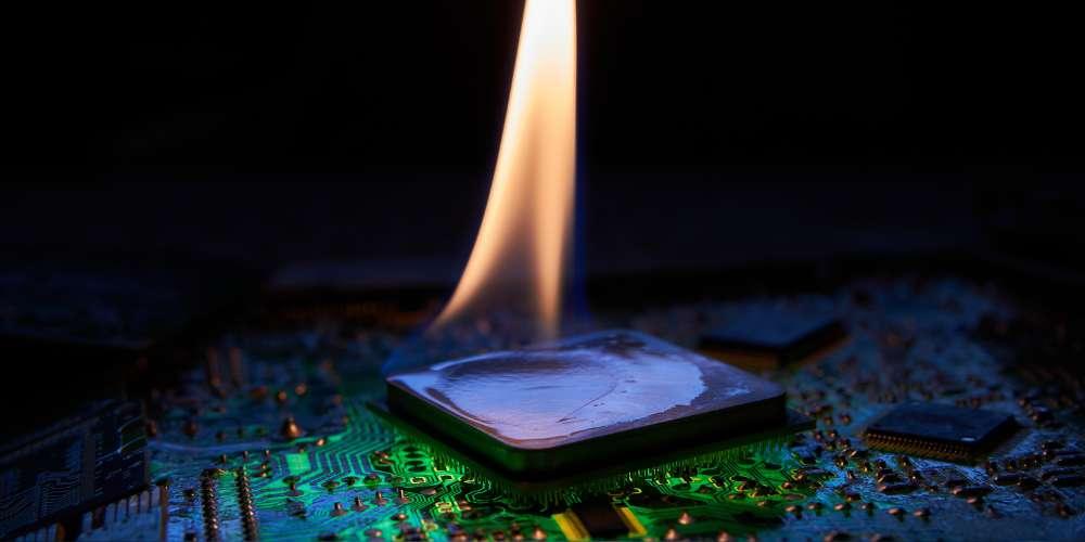
That's why the problem for AI chips is not that they cannot perform calculations, but that they might overheat and break down before finishing the calculations.
The CPUs and GPUs in traditional computers also generate heat, but their power consumption is relatively limited, and radiators can gradually dissipate the heat out.
For today's high-end AI accelerators, the power consumption of a single AI chip has entered the kilowatt era.
What's more troublesome is that a large number of transistors and computing units inside the AI chip are concentrated in the core area, leading to extremely high heat density.
The same 1 kilowatt of heat distributed across an entire table is completely different from the same amount of heat squeezed into a space the size of a fingernail.
At this point, traditional copper obviously can no longer meet the demand, and people need to find new alternative materials.
02
Why is the Henan diamond industry targeted in particular?
So engineers started looking through material libraries, and finally found a seemingly absurd answer: diamond, the very same material in the famous slogan "A diamond is forever".
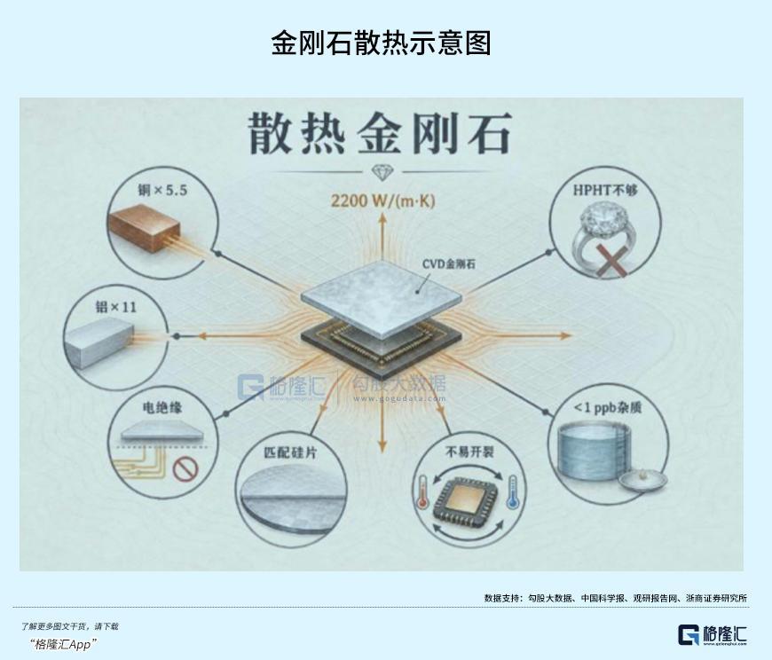
Why diamond? Because diamond has an incredibly outstanding physical property: extremely high thermal conductivity.
The thermal conductivity of high-quality diamond can reach more than 2000W/(m·K), which is 5 times that of copper and 10 times that of silicon.
Moreover, diamond not only has excellent thermal conductivity, but also features high hardness, high temperature resistance and stable chemical properties, giving it very unique material advantages in high-power and high heat flux density scenarios.
To put it simply: you can attach it to the hottest part of the chip to dissipate heat right where it is needed most.
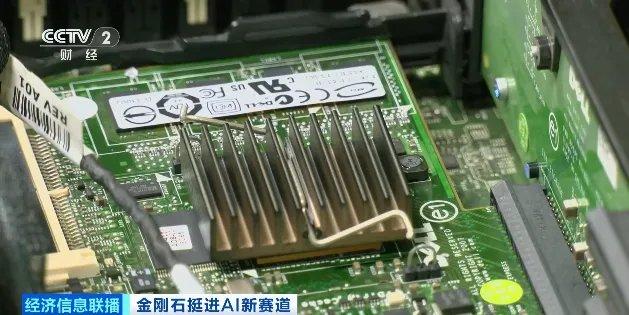
From this perspective, what NVIDIA wants is never the shiny large gem-quality diamonds, but ultra-thin diamond materials nearly as thin as cicada wings, which can be directly integrated into the chip packaging system to undertake heat diffusion and heat dissipation tasks.
This material is commonly called: diamond heat sink wafer. The name sounds simple, but it is extremely difficult to manufacture.
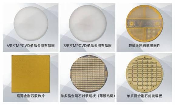
First of all, the material must be pure enough.
Chip heat dissipation cannot be done with ordinary industrial diamonds. Defects and impurities inside the material will affect the thermal conductivity performance.
Secondly, the size of the material must be large enough.
In the past, industrial diamonds with a size of a few millimeters or centimeters were enough for use. But as chip packaging sizes keep growing, heat sink materials must also evolve to larger sizes accordingly.
After that, there are a bunch of other requirements for thickness, flatness, surface roughness, thermal expansion matching, packaging reliability and so on.
It is not enough just to "make diamonds". You have to make diamonds thin enough, flat enough, pure enough, and be able to produce them stably in batches.
This is exactly what Henan's lab-grown diamond industry is best at.
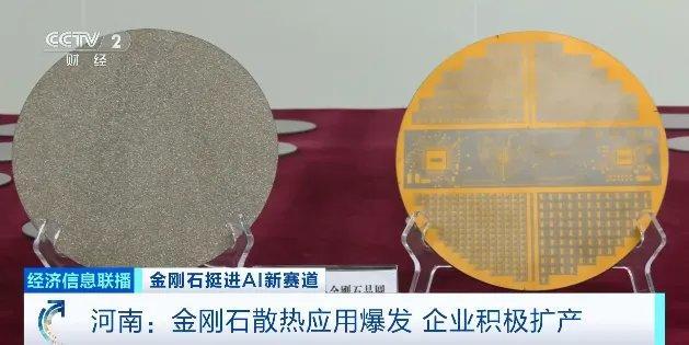
Decades ago, Henan had already started researching synthetic diamond as an industrial material.
After decades of industrial accumulation, a fairly complete industrial chain has taken shape, covering diamond synthesis equipment, raw materials, micropowder processing, CVD diamond and various functional materials.
Therefore, as soon as the demand for AI heat dissipation emerged, Henan's factories could immediately start production.
For example, Henan Liliang Diamond has already laid out diamond heat dissipation materials, and its related products have passed NVIDIA's laboratory verification, and have been included in the BOM list of HGX modules.
On the other hand, Huanghe Whirlwind is also continuously deploying CVD diamond heat sink materials, and is advancing the 8-inch diamond heat sink wafer production line.
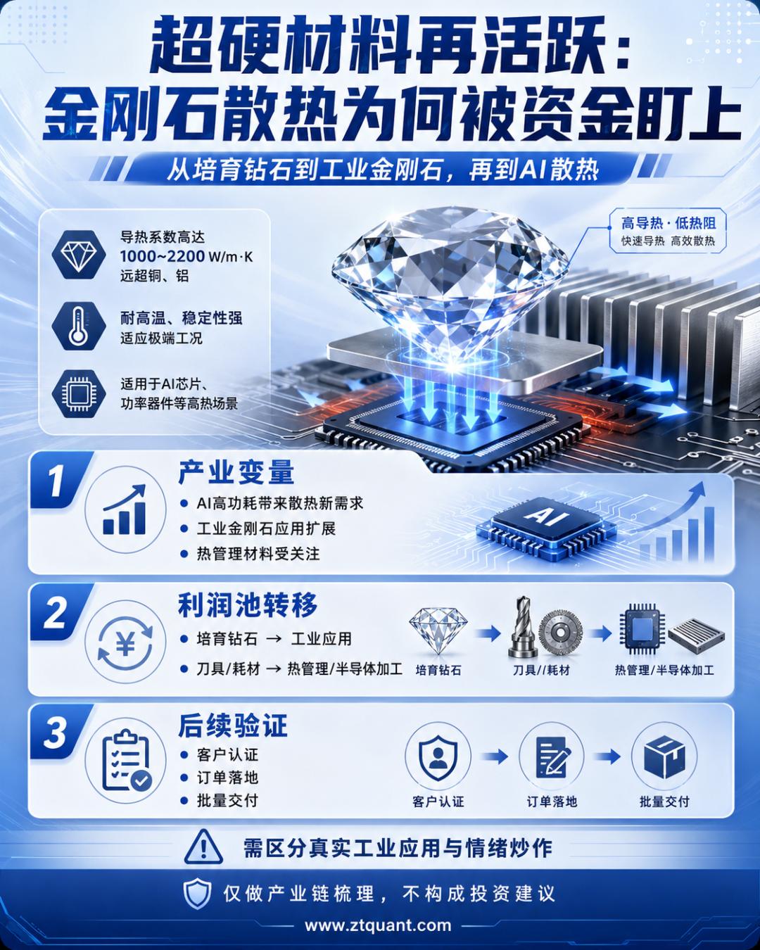
As we all know, the chip industry attaches great importance to wafer size. A larger size means a larger effective processing area in a single production run, and also requires materials to have higher consistency and more stable mass production capacity.
Here is a little-known fact: diamond was originally developed to meet industrial demands. The diamond that later became popular in the consumer market is more like a "side business".
Therefore, when Henan diamond enterprises are developing 8-inch diamond heat sink wafers, they are not suddenly crossing over from the "jewelry business" to the chip industry.
They were originally industrial material manufacturers, and this time, AI has brought this mature traditional craft into the semiconductor industrial chain with much higher added value.
03
All industries in the United States have long coveted this material
At this point, if you think Henan's diamond industry is targeted by NVIDIA just because AI chips are overheating, you are still underestimating the huge value of this small material.
In fact, the United States has long been eyeing it, because the capabilities of diamond go far beyond cooling down chips.
It is hard, high temperature resistant, excellent in thermal conductivity, and also has special properties in optics, electricity and other aspects, making it a precious material in high-end fields such as aerospace, radar and laser technology.
For example, the infrared dome at the front end of a missile.
This part looks unremarkable, but has extremely strict requirements: it must allow infrared signals to pass through smoothly, and at the same time withstand high temperatures, friction and impact caused by several Mach speeds during high-speed flight.
Diamond happens to combine high hardness, high temperature resistance and excellent infrared optical performance, making it an important candidate material for high-end infrared windows.
Take radar as another example. High-performance systems such as the US Navy's SPY-6 radar and Patriot missile radar all use gallium nitride devices.
Gallium nitride devices have high power and high frequency, but their heat generation also rises sharply as the power increases. Diamond is just the "all-rounder" in the heat dissipation field.
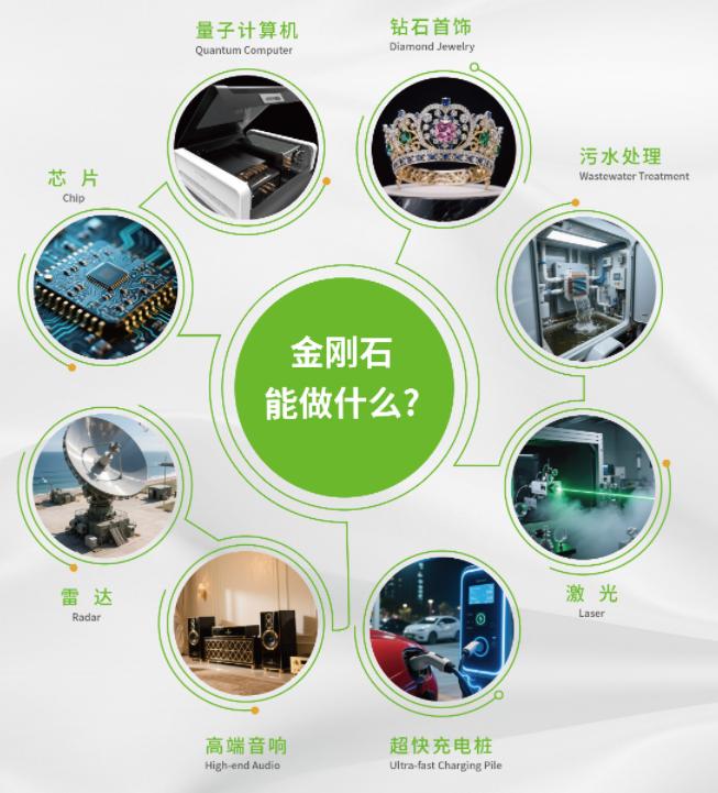
In addition, shipborne infrared search systems, early warning devices, laser weapon windows, aircraft optical windows, and superhard cutting tools for processing aerospace titanium alloys all rely heavily on diamond.
In other words: AI needs it, the military industry needs it, and the aerospace industry also needs it.
At this point, looking back at China's synthetic diamond industry, the situation becomes very interesting.
On October 9, 2025, the Ministry of Commerce of China implemented export controls on items related to superhard materials. Only 4 days later, the US Department of Defense announced that it would invest more than 1 billion US dollars in the procurement of critical minerals.
However, natural diamonds can only serve as an emergency stopgap, and their output cannot support such a huge industrial demand at all.
Cubic boron nitride and tungsten carbide have also been used as alternatives, but the problem remains: being a possible substitute is completely different from being able to fully meet the demand.
In some scenarios with extremely high performance requirements, it is very difficult for alternative materials to fully match diamond in key indicators such as thermal conductivity and hardness.
After going around in circles, the United States found that the most reliable solution is still: to produce it on its own.
It sounds simple, but building factories, purchasing equipment, and launching production lines is far more complicated than imagined.
It is worth noting that several major diamond giants in China have a development history of more than 10 years, and some even 30 to 40 years.
It took decades of efforts to gradually build up the complete system covering equipment, processes, materials, talents and supply chains.
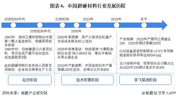
If the United States starts from scratch, it will optimistically take 5 to 10 years to achieve truly stable and large-scale production.
Moreover, building a factory is only the first step. "Being able to produce" does not equal "being able to produce high-quality diamonds". Especially when entering high-end fields such as AI chips, aerospace and military industry, there are extremely high requirements for purity, size, defect rate, consistency and processing accuracy.
This requires a large amount of R&D investment, and more importantly, long-term accumulated professional knowledge.
There is even a more troublesome problem: talent. Where to find people who understand materials? Where to find people who understand equipment? Where to find people who master diamond synthesis and processing techniques?
In addition, there is the supply chain. The whole process of moving diamond from the laboratory to mass production cannot be completed by a single company working behind closed doors. It requires cooperation between upstream and downstream players.
The most impressive advantage of Henan is exactly this: a highly dense industrial cluster has already taken shape here.
It can be seen that the diamond industry in Henan has made diamond giant De Beers lower its stance, attracted NVIDIA to come for cooperation, and also made the Pentagon anxious.
04
Final notes
After the news came out, many people online joked that Henan's lab-grown diamond, which young people used to look down on, has finally got a new lease of life thanks to the AI boom.
It seems that any industry that gets related to AI can take off immediately.
In the past two years, we have seen many similar stories: AI server prices are rising, optical module prices are rising, liquid cooling prices are rising, copper prices are rising, and now even diamonds are drawn into the AI industrial chain.
But we think the opposite is true: it is not that synthetic diamond is riding on the AI trend, but that synthetic diamond is saving the increasingly overheating AI chips.
It can be seen that truly competitive industries are never afraid of being underestimated.
Feel free to share your thoughts in the comment section: what other traditional industries that seem completely unrelated to AI are secretly benefiting from the AI dividend?
Maybe the next industry that will suddenly be boosted by AI is hidden in a place you never expected.
References:
China Central Finance, Huashang Taolue and other online sources
This article is from the WeChat official account "Tech Fox" (ID: kejihutv), written by Lao Hu, edited by Bu Chi Maiyatang, published with authorization from 36Kr