NPO has emerged as a new force that has suddenly risen to prominence.
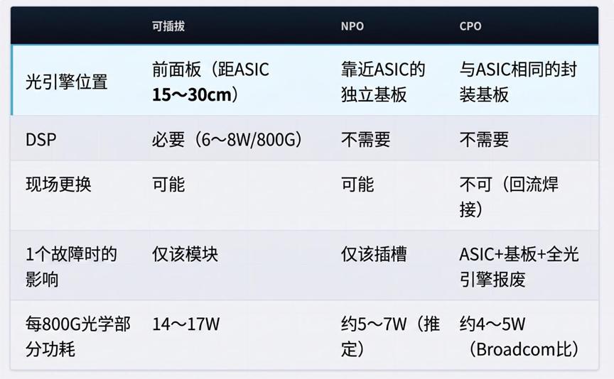
Open the data center rack, and you will see rows of optical transceivers arranged on the front panel of the switch. In AI clusters, it is a common configuration for a single switch to be equipped with 144 800G-compatible QSFP-DD modules. However, this configuration has the problem of structural inefficiency. The distance from the transceiver on the front panel to the switch ASIC chip is 15 to 30 cm. When a 200G/lane signal travels along this copper wire, it will experience significant attenuation, requiring a DSP (Digital Signal Processing) chip at the receiving end to recover the signal. A single 800G module consumes 14 to 17 watts, of which 6 to 8 watts are consumed by the DSP chip. That is to say, a considerable part of the power consumption in the traditional pluggable optical module is not directly used for photoelectric conversion, but is consumed in the conditioning, equalization and transmission of high-speed electrical signals.
Shortening this distance will eliminate the need for DSP. This concept emerged as early as the mid-2010s. Co-packaged Optics (CPO) integrates the optical engine (a set of components that convert electrical signals into optical signals) and the switch ASIC on the same substrate. This design greatly shortens the high-speed electrical connection distance between the ASIC and the optical engine, thereby significantly reducing the loss caused by copper interconnection. Broadcom announced that CPO can reduce the power consumption of optical systems by 65-70%. The power consumption of NVIDIA's 1.6T link has been reduced from about 30 watts per link to 9 watts.
In theory, CPO seems to be the optimal solution. The problem is that there is a gap between theory and mass production.
9% Yield Rate Reveals the Truth
In the CPO manufacturing process, the optical engine is mounted on the ASIC packaging substrate through reflow soldering (thermal welding). The fiber alignment accuracy reaches the sub-micron level. If you want to reinstall the installed optical engine, you need to reheat it to 220-260°C, and the heating position is a few millimeters away from the ASIC, while the fiber alignment accuracy cannot withstand the second thermal damage. In other words, if one of the 32 optical engines is defective, the ASIC, the substrate and all remaining optical engines must be scrapped.
In its June 2026 research report "Powered Down, Lights Off", SemiAnalysis assumed that the implementation yield of each optical engine is 95%, and calculated that the combined yield is 0.95^32 ≈ 0.1932. In other words, under the extremely simplified model that 32 optical engines are independent of each other and each has a yield of 95%, the combined yield of all 32 engines passing the test is about 19.3%. This means that only one-fifth of the engines can work normally. This figure has had a significant impact on the market. On June 9, in the US market, Applied Optoelectronics (AAOI) share price fell by about 17% in one day, Lumentum by about 8%, Coherent by about 11%, and Marvell by about 7.6%.
GlobalSemiResearch immediately issued a rebuttal statement, pointing out that the calculation ignored the yield improvement brought by screening, grading and the redundant engines designed by NVIDIA for Spectrum-X. Morgan Stanley also said in a report on June 10 that it did not deny the CPO technology roadmap, but only lowered its 2027 optical engine shipment forecast from the previous 20 million to 30 million units to 6 million to 7 million units.
The focus of this debate is not "Is CPO bad?", but "When and at what scale can CPO be used?". SemiAnalysis has postponed the horizontal expansion shipment of CPO to 2027, and the full mass production to 2028-2029. The adjustment of this timetable opens a window for the exploration of other architectures.
The All-round Advantages of NPO
Near-packaged Optics (NPO) is between Co-packaged Optics (CPO) and the pluggable design. The optical engine is installed on an independent engine board, not on the ASIC's packaging substrate, and is placed close to the ASIC. When the electrical link is short enough and the loss is low enough, the DSP used in traditional pluggable optical modules to compensate for the loss of long-distance electrical links can be reduced or even eliminated in some architectures. However, a key difference between it and CPO is that the engine is connected through a socket and can be plugged and unplugged on site.
On August 10, SemiAnalysis summarized three advantages of NPO on the X-thread forum: on-site maintainability, the failure spread (influence scope) is limited to a single slot, and the assembly process is simplified because the optical engine and ASIC adopt independent packaging. This structure avoids the challenges in production and reliability, while retaining most of the performance advantages of CPO.
At the OFC exhibition in March 2026, Broadcom released its NPO product line based on 3.2T VCSEL. According to the company's blog, the energy efficiency of this NPO engine is about 1 pJ/bit, which is 5 to 10 times higher than the silicon photonics method with the usual energy efficiency of 5 to 10 pJ/bit. After deploying 18 engines, the escape bandwidth density exceeds 0.6 Tbps/mm, and the total escape bandwidth reaches 73.7 Tbps (128 Gbps/lane). VCSEL has decades of mass production experience, and its field-verified failure rate (FIT) is less than 0.1.
The Gears of Standardization and Mass Production Start to Turn
Even with an excellent architecture, widespread application cannot be achieved without the support of the ecosystem. On March 12, 2026, on the occasion of the OFC conference, six companies including Ciena, Coherent, Marvell, Molex, Samtec and TeraHop jointly signed the Open CPX MSA (Multi-Source Co-Packaged Agreement). This agreement aims to develop common specifications for socket-mounted optical engine interfaces covering NPO and CPO. This will standardize the mechanical structure, thermal design, electrical pinout and management interface of the connectors, so as to ensure interoperability between products of different manufacturers.
Vladimir Kozlov, CEO of LightCounting, said when announcing the establishment of the organization, "It is expected that the annual shipment will exceed 100 million units in five years", while the shipment of CPO/NPO is expected to be less than 1 million units by 2025. Without standardization, such a huge growth (even more than 100 times) is impossible to achieve.
Demand is also changing. At the IPEC webinar held in May 2026, Alibaba revealed that it plans to complete the beta test of its 3.2T NPO and start pilot operation in the third quarter of the same year. Its goal is to complete the system-level debugging of 6.4T NPO alpha samples by September 2027. Tencent has also completed the verification of its 3.2T VCSEL NPO and silicon photonics NPO, and plans to carry out pilot deployment in the fourth quarter of 2026. Ranovus has delivered NPO modules to US cloud companies, but it is expected that the official announcement will not be made until the OFC exhibition in 2027.
In terms of supply chain, Foxconn Interconnect Technology has started mass production of solderless LGA-to-LGA sockets and pluggable laser source cages for Broadcom's Bailly since May 2025. Lasers are mainly designed to be placed outside the package, whether it is CPO or NPO, and the ELSFP standard (hot-swappable external laser module) formulated by OIF in August 2023 serves as a general foundation.
Why NVIDIA's CPO Presents NPO Features
NVIDIA's Quantum-X Photonics InfiniBand switch has been announced to start mass production deployment. It provides 144 800G ports, equipped with 18 silicon photonic engines and 18 detachable external laser modules to provide light sources. NVIDIA calls it "CPO".
However, the engine can be easily removed from the package, and the laser can be slid out from the front panel, which is exactly the maintainability advantage of NPO recognized by SemiAnalysis. LightCounting confirmed in a July 2026 research report that the industry generally believes that CPO and NPO will coexist, and pointed out that if NVIDIA uses NPO as an option, the development cycle will be shortened, and initial deployment may be seen as early as next year.
Broadcom will deploy both architectures in parallel. The 51.2T Bailly CPO switch has been mass-produced at Micas Networks since 2024. The 102.4T Tomahawk 6 Davisson switch has started shipping to customers in October 2025. In addition, Broadcom will separately provide 3.2T VCSEL NPO switches to meet the needs of customers who require high-density switches but do not want to perform soldering.
Meta's reliability verification is also steadily advancing. In Meta's high-temperature laboratory environment, Broadcom's CPO system recorded zero link jitter (instantaneous interruption) during a cumulative operation of 1 million hours (equivalent to 400G port hours). Broadcom announced this result in October 2025, and released relevant details at ECOC in the same year and OFC in 2026. At OFC 2026, Meta put forward the standard that "to be attractive, optical technology must be comparable to electrical solutions in terms of cost and energy efficiency, while providing reliability and performance".
TSMC COUPLE Plays a Key Role
The end of the NPO "transition phase" largely depends on the progress of TSMC's COUPE (Compact Universal Photonic Engine) platform.
As mentioned above, it is well known that the computing power of current AI chips has been extremely powerful, but when data is transmitted between chips, it still relies on copper wires for conduction. The transmission speed and energy consumption of copper wires are gradually unable to keep up with the growth rate of computing power. The core idea of COUPE is to use optical signals to transmit data, and move the position of photoelectric conversion from the remote optical module into the chip package, greatly shortening the path that signals have to travel.
COUPE integrates two types of chips, one is responsible for processing electrical signals (Electronic Integrated Circuit, EIC), and the other is responsible for processing optical signals (Photonic Integrated Circuit, PIC). The two are directly stacked up and down through TSMC's 3D stacking technology, connected face to face, eliminating the loss of signals bypassing the circuit board in traditional solutions.
TSMC stated that compared with the pluggable solution on the circuit board, integrating the COUPE optical engine directly on the packaging substrate can achieve 4 times power efficiency and reduce latency by 90%; if COUPE is further placed on the Interposer, the performance can be increased to 10 times power efficiency and 95% latency reduction.
The COUPE technology adopts the SOIC stacking method to directly stack the electronic chip and the photonic chip, thereby minimizing the impedance between the chips. The first-generation pluggable COUPE will be mass-produced in 2026. The second-generation COUPE adopts 6.4T CPO packaging and is expected to be mass-produced around 2027. The third-generation product will fully integrate the optical components inside the processor package.
TSMC's COUPE bandwidth density roadmap predicts that the bandwidth density will increase by 8 times within four years, from 0.5 Tbps/mm in 2026 to 4 Tbps/mm in 2030. If this plan is realized, the role of NPO will be limited to a transition period of two to three years.
However, if the full mass production scenario predicted by SemiAnalysis in 2029 is close to reality, NPO will continue to meet market demand until the end of the 2020s. In this case, it will put additional pressure on the photonics supply chain, which is already stretched in terms of laser and packaging capacity. At the OCP Asia Pacific Summit, Nicole Tien from ASE pointed out that there are currently no wafer-level testing standards and simulation infrastructures to promote CPO to a multi-vendor market. NVIDIA's CPO mass production is the result of in-depth bilateral cooperation and R&D with TSMC, and there are currently no conditions to extend these results to the entire industry.
It is generally believed in the industry that the ultimate form of optical interconnection is CPO. The question is, who will choose this path, when to achieve it, and at what scale? At least from the current product roadmap and customer verification situation, NPO is rapidly moving from technical verification to large-scale deployment, becoming a more certain answer.
This article is from the WeChat official account "Semiconductor Industry Watch" (ID: icbank), author: Editorial Department, authorized by 36Kr for release.