Meta's first training chip has officially been unveiled.
In March this year, Meta disclosed plans for a series of chips including the MTIA 300. Recently, they finally unveiled the first chip in this roadmap to the public.
As introduced, MTIA 300 is Meta's first AI training chip optimized specifically for Deep Learning Recommendation Models (DLRM). Unlike GenAI training, DLRM training does not require extremely high floating-point computing performance, but demands large-capacity memory, high network bandwidth, and frequent collective communication; this combination usually leads to low accelerator utilization. MTIA 300 addresses these challenges through three key innovations:
A network interface chipset with 12×800 Gbps RDMA network adapters built in, which ensures high network performance and eliminates PCIe overhead;
A dedicated message engine for collective offloading, which delivers throughput comparable to that of the compute engine while only occupying one-third of the chip area;
Near-memory computing, which places the message engine close to HBM, caches, and I/O, and is equipped with dedicated hardware to accelerate reduction-based collective operations such as ReduceScatter.
Although MTIA 300 was originally designed for DLRM, these widely applicable design principles also apply to subsequent MTIA series chips optimized for GenAI models (MTIA 400, 450, and 500).
As far as we know, MTIA 300 is the first accelerator with a built-in network adapter chip and a general-purpose collective offloading engine, capable of enabling efficient scale-up and scale-out communication. In addition, MTIA 300's moderate floating-point computing performance, higher HBM bandwidth and capacity were initially optimized for training DLRM models, but these features also make it suitable for GenAI inference. Performance evaluations show that MTIA 300 delivers performance comparable to GPUs of the same generation, while also having cost advantages.
Introduction
Artificial intelligence workloads continue to grow rapidly across the entire industry. At Meta, products such as Facebook and Instagram rely on Deep Learning Recommendation Models (DLRM) to deliver personalized content, including advertisements, short videos, and friend feeds. This growth has driven Meta to independently develop artificial intelligence chips. We previously launched MTIA 1 and MTIA 2i (also known as MTIA 100 and 200), both of which are optimized for DLRM inference, and hundreds of thousands of MTIA 2i chips have been deployed so far.
This article will introduce the next step in this development journey: Meta's first training chip, MTIA 300.
Meta supports two major categories of artificial intelligence workloads: GenAI and DLRM. DLRM training differs from GenAI training: it requires fewer floating-point operations (FLOPS), but demands larger HBM capacity, higher network bandwidth, and more frequent communication. This combination usually leads to relatively low accelerator utilization. Unlike general-purpose GPUs, MTIA 300 is optimized for DLRM, and its design is intentionally different from GPU architectures to reflect this focus.
To clarify the design motivation of MTIA 300 for Deep Learning Recommendation Models (DLRM), we first summarize the workload characteristics. DLRM usually applies multi-layer perceptrons (MLP) to dense features (such as user age), applies embedding tables to sparse categorical features (such as post IDs), and connects them through dense interaction layers. The dense components require high floating-point computing performance (FLOPS) (though far lower than GenAI), while the sparse components need irregular access to extremely large embedding tables and are usually limited by memory or instructions. Since embedding tables usually exceed the memory capacity of a single accelerator (sometimes accounting for more than 99% of model parameters), DLRM adopts hybrid parallelism in training: data parallelism is used for dense layers, while embedding tables are sharded by table or by row for sparse layers. This approach enables training of large models without sacrificing the computational efficiency of dense layers.
The combination of data parallelism and model parallelism for different model components introduces complex communication patterns. In terms of data parallelism, each accelerator receives a local batch and performs AllReduce operations to synchronize gradients. Model parallelism exchanges features through AllToAllv collectives and redistributes results during forward and backward propagation. In addition, many DLRM algorithms use the distributed Shampoo optimizer for dense components, which adds AllGather operations during the optimization phase. Efficient execution of these collectives is critical to achieving high performance.
Since DLRM places higher demands on the communication data path, MTIA 300 integrates the following features to address this challenge:
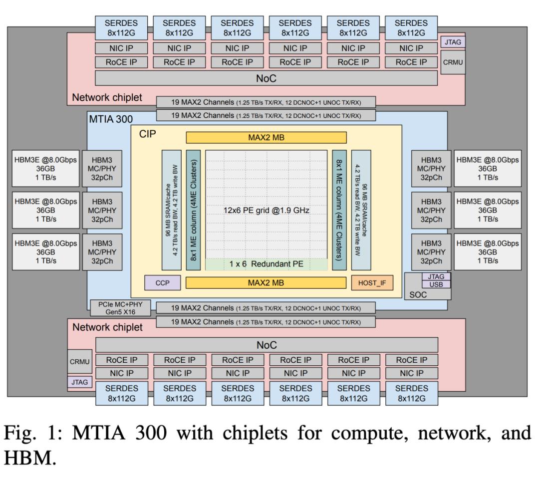
• Built-in network adapter chip: MTIA 300 adopts a chiplet architecture, embedding two network adapter chips that contain a total of 12 highly optimized 800Gbps RDMA network adapters. The built-in network adapter avoids PCIe overhead between the accelerator and the network adapter, and the network adapter can be flexibly used for scale-up or scale-out networks.
Collaborative offloading: In GPUs, the compute engine and host CPU handle collective operations, which is usually inefficient. In contrast, MTIA 300 uses a dedicated message engine to provide the same communication throughput for these operations as the compute engine, while only occupying one-third of the chip area.
Near-memory computing: The compute engine and the message engine share the on-chip network for memory and I/O access. To avoid congestion caused by high-bandwidth collective operations, the message engine is placed at the edge of the chip, close to HBM, caches, and I/O ports. The near-memory computing logic block of the message engine provides high throughput for all reduction-based collective operations, including Reduce, AllReduce, and ReduceScatter.
In addition to outlining the unique hardware features and overall architecture of MTIA 300, we also describe the software stack, focusing on the collectives library, which provides a familiar interface while effectively utilizing MTIA's dedicated message engine and built-in network adapter to achieve efficient communication.
Although many GPUs and AI ASIC chips have been reported, our experience shows that DLRM has some unique requirements that have not been addressed in previous research. As far as we know, MTIA 300 is the first accelerator with a built-in network adapter chip and a general-purpose collective offloading engine, which avoids the inefficiency of using the compute engine for collective computing, and enables flexible network configurations that meet both scale-up and scale-out requirements. In contrast, although the sparse cores of TPU can also offload remote access to embedding tables, they are dedicated to non-RDMA, non-switched torus networks, and lack a general-purpose collective library interface, which limits their application in other industry accelerators that are usually built based on RDMA and similar collective library interfaces.
Although the notable features of MTIA 300 - built-in network adapter chip, collective offloading, and near-memory computing - were originally designed for DLRM training, these design principles still have broad applicability and have been adopted by subsequent MTIA series products optimized for GenAI models. The development of MTIA 300 started several years ago, aiming to compete with H100 and H200 GPUs, while its successor MTIA 400 is designed to compete with GB300 GPUs. In addition, the upcoming MTIA 450 and 500 aim to surpass future GPUs in GenAI inference performance and reach the industry-leading level.
MTIA 300 Architecture
Figure 1 shows an overview of MTIA 300, which adopts a chiplet architecture. To highlight its unique features, we first compare MTIA 300 with MTIA-2i, and then with GPUs.
A. Comparison of MTIA 300 with MTIA-2i and GPUs
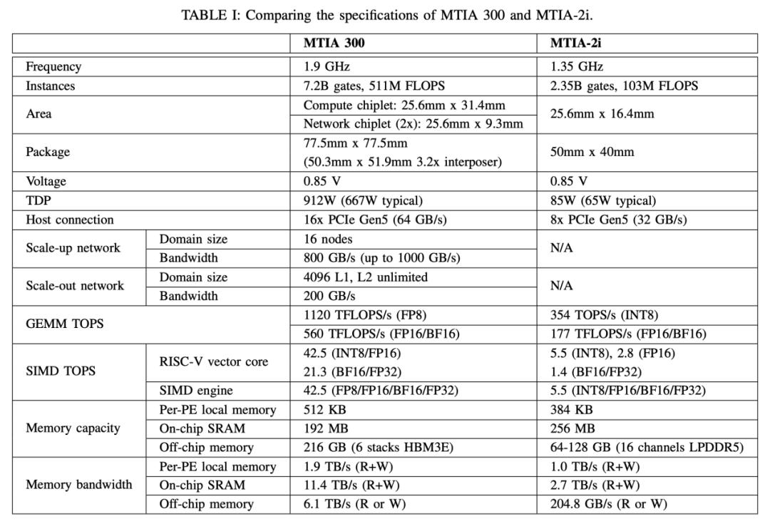
Table I compares the specifications of MTIA 300 and MTIA-2i. MTIA-2i is designed for inference, while MTIA 300 is designed for training. MTIA 300 introduces multiple improvements: the area is increased by about 3 times, the thermal design power (TDP) is increased by about 10 times, liquid cooling (instead of air cooling) is adopted, HBM3E (instead of LPDDR) is used, FP8 computing (instead of INT8) is supported, BF16 FLOPS is increased by more than 3 times, 2.5D CoWoS packaging is used, the size of the compute die is the same as the reticle size, the network chip supports RoCE, and a message engine for offloading collective communication is added. Notably, the SIMD computing performance of FP32 has been increased by more than 6 times, making the ratio of GEMM to SIMD reach 16:1, while the ratio of MTIA-2i is 32:1; this increase is quite considerable considering the growing and diverse demand for non-GEMM computing in training (such as table-based batch embedding forward/backward iterations and optimizers).
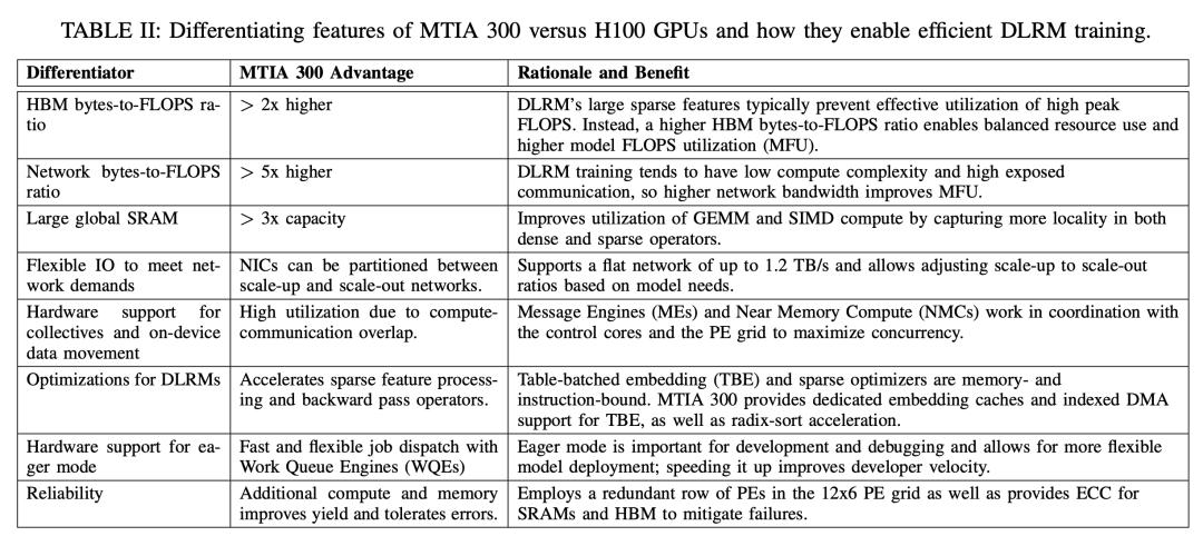
Unlike general-purpose GPUs, MTIA 300 is optimized for DLRM. Table II highlights its differences from H100 GPUs. Notably, MTIA 300 weakens the peak floating-point performance, while focusing on improving HBM bandwidth and network performance, featuring a built-in network adapter chip and dedicated hardware support for collective communication offloading.
B. MTIA 300 Compute Die
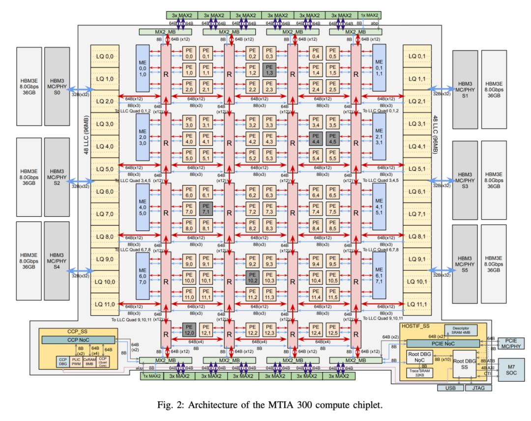
Figure 2 shows the architecture of the MTIA 300 compute die. It consists of a 12×6 grid of Processing Elements (PE) for executing computing tasks, and contains 16 Message Engines (ME) for performing collective operations. On the east and west sides, SRAM banks can be used as Last Level Cache (LLC) or Last Level Scratchpad (LLS). Each side is connected to 3 stacks of 12-layer HBM3E. Processing elements, as well as processing elements and on-chip/off-chip memory, are connected through a mesh interconnect.
Network on Chip (NoC): NoC is a two-dimensional router mesh structure that connects processing elements and message engines within the main grid. It also connects the compute die to the control and host interface modules, as well as chip interface IP modules located on the north and south sides, which are connected to the network die. NoC provides data, control, utility (such as register access and debugging), synchronization, and reduction channels. To improve performance and scalability, we introduce cluster routers to locally connect six PE nodes, thereby reducing total hop count latency. Unlike MTIA-2i, the compute die does not use a memory crossbar; instead, the Network on Chip (NoC) handles memory bank selection routing. It adopts the Lrouting algorithm - moving along one dimension (such as the X axis) first, then along the other dimension (Y axis) - to distribute traffic evenly across the entire grid, and uses virtual channels to avoid deadlocks.
Host interface: MTIA 300 provides a high-performance host interface that supports PCIe, DMA, and secure boot processors. It contains interfaces for the host to manage the compute and network dies, as well as debug interfaces.
Control core: This is a RISC-V quad-core SMP core, responsible for coordinating the execution between PEs and MEs. It contains associated context RAM, mailbox registers, and MSI-X interrupts.
Redundancy: To improve the yield of lithography-limited chips, the compute die contains a redundant row of PEs. Since PEs occupy the largest area and distributed memory, and considering the east-west organization of memory and the routing paths of the Network on Chip (NoC), adding a redundant row is the simplest solution. Each PE column can tolerate one faulty PE by replacing the corresponding PE in the redundant row. This configuration is completed at startup, is transparent to software, and does not affect the performance of NoC.
C. Processing Element (PE)
Figure 3 shows the internal architecture of the Processing Element (PE). Each PE contains two RISC-V cores, fixed-function units for accelerating computing and data transmission, and internal memory that connects all components through a memory bridge.
Memory Bridge (MB): The memory bridge provides data and configuration connections between all components in the PE through the internal Network on Chip (NoC). It also contains peripherals such as interrupt controllers, machine timers, and debug/trace modules.
Local memory: Each PE contains 512 KB of fast local storage (LS). LS is managed by software and divided into circular buffers (CB) of controllable size.
RISC-V cores: The RISC-V cores execute application code and issue commands to the command processors of the fixed-function units. MTIA 300 has two 64B-wide vector cores, which provide additional SIMD throughput and a symmetric programming model, allowing the same code sequence to run on either core. MTIA uses an asynchronous dataflow execution model. Programmers write a kernel that generates a series of custom instructions for the fixed-function units, performing data movement and computation while resolving dependencies.
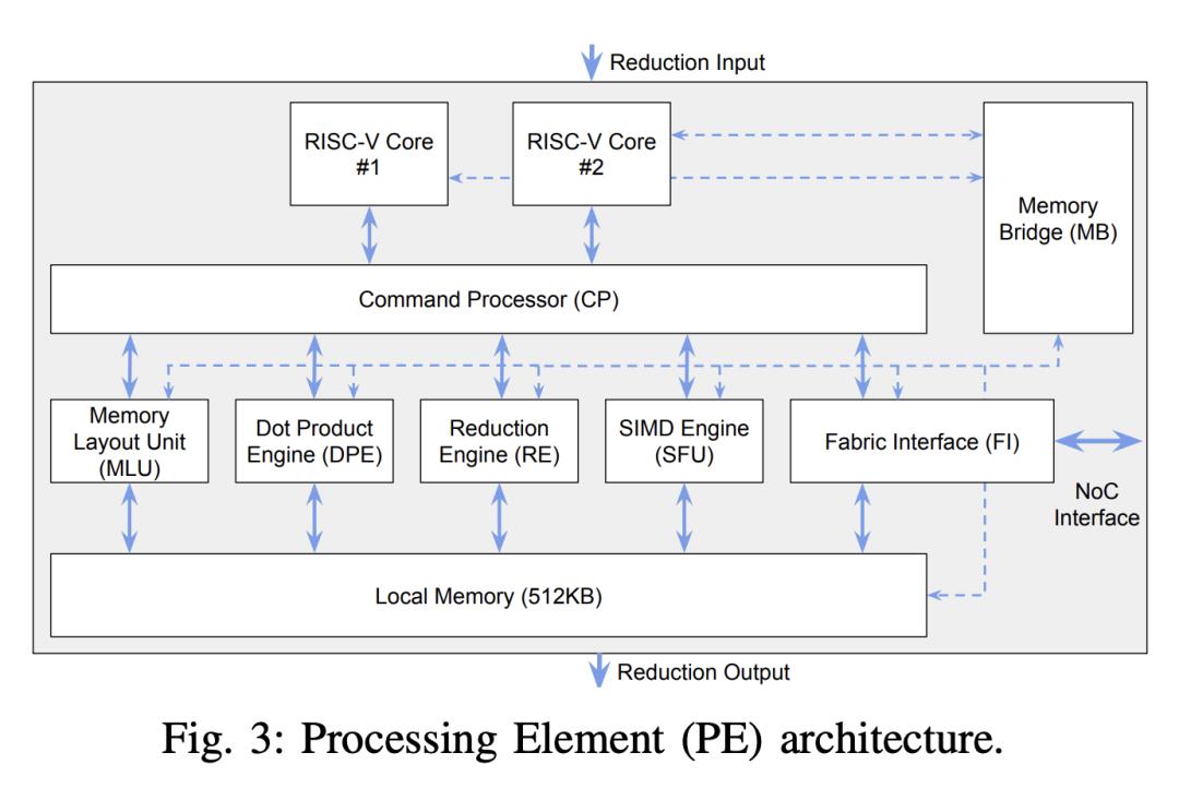
Memory Layout Unit (MLU): The MLU performs memory layout transformations, including transposition, reshaping, slicing, and concatenation.
Dot Product Engine (DPE): The DPE performs General Matrix Multiplication (GEMM) operations for the forward and backward propagation of training. It processes two input tensors: the first tensor is read and cached in the DPE, while the second tensor is streamed from the LS and performs dot product operations with all rows of the first tensor. The DPE contains two 32×64B×32 Multiply-Accumulate (MAC) modules, with a total throughput of 7.82 TFLOPS per PE, supporting FP16/BF16 inputs and FP32 outputs. It also supports FP8 inputs (S1E4M3 or S1E5M2 formats) and TF32 inputs, which is very useful for certain ranking and recommendation application scenarios that require higher precision.
Reduction Engine (RE): The RE stores intermediate matrix multiplication results from the DPE and performs inter-PE reduction operations through a dedicated reduction network. It can receive and accumulate results before forwarding them to the next PE or SIMD engine for further processing.
SIMD Engine (SFU): The SFU supports quantization, element-wise operations, and nonlinear functions. It consists of an execution pipeline containing a floating-point ALU and a Look-Up Table (LUT) for approximating nonlinear functions. The SFU can receive input from the RE or read data directly from the LS. For training, we removed INT8 support and added FP8, FP16, BF16, and FP32 support. The SIMD width is increased from 32 elements per cycle to 128 elements to achieve a 16:1 GEMM:SIMD ratio (half that of MTIA-2i), which reflects that a large part of the computation is consumed by non-GEMM operations. Two RISC-V cores provide additional SIMD throughput.
Based on the requirements of DLRM training, we have made multiple improvements to the SFU, including increasing the throughput of nonlinear operations on high-precision data types, and adding support for min/max, clamping, and stochastic rounding. MTIA 300 also supports hardware-accelerated radix sort to speed up backward embedding operations. During the forward propagation process, sparse offsets and indices are packed