All are eyeing EUV lithography machines
EUV lithography systems, which were once affordable only for TSMC, Samsung and Intel, are now appearing on the capacity expansion lists of Nanya Technology and Winbond Electronics. Meanwhile, a group of startups founded just two or three years ago are attempting to bypass traditional EUV lithography machines by using X-rays, particle accelerators and even helium atoms. We also reported a few days ago that Elon Musk seems to intend to put FEL into mass production. For details, please refer to the article "Elon Musk, to Disrupt EUV Lithography Machines?"
It can be seen that seemingly overnight, almost everyone can access and use EUV technologies. Is the threshold of EUV really disappearing?
Major Players of EUV Lithography Systems
At present, the players that have truly achieved large-scale mass production of EUV are still highly concentrated, and the core players remain TSMC, Samsung, Intel, SK Hynix and Micron.
Among them, TSMC is one of the manufacturers with the earliest commercialization of EUV and the largest application scale. In 2019, TSMC officially introduced EUV in the N7+ process and realized commercial mass production. Subsequent advanced nodes such as N5 and N3 further increased the number of EUV exposure layers, and EUV gradually evolved from a few initial critical layers to a core tool for advanced logic manufacturing.
Samsung Electronics is advancing EUV on two product lines of advanced logic and DRAM at the same time. In addition to advanced process foundry services, Samsung has introduced EUV into the mass production of 14nm-class and 12nm-class DRAM, enabling EUV to gradually expand from advanced logic to memory chip manufacturing.
Intel's EUV introduction was relatively late, but the promotion speed is very fast. Intel 4 has become its first process to adopt EUV on a large scale, and subsequent Intel 3 and 18A continue to expand the application. At the same time, Intel is also one of the chip manufacturers that first received and deployed ASML High-NA EUV equipment, conducting technical verification in advance for next-generation processes such as 14A.
Among memory manufacturers, SK Hynix began to introduce EUV in the mass production of 1a nm-class DRAM in 2021, and continued to expand the scope of application thereafter. In 2025, the company installed High-NA EUV equipment at the M16 fab in South Korea, bringing the new generation of EUV technology into the DRAM R&D and future mass production system in advance.
Micron is the one among the three major DRAM manufacturers that formally introduced EUV relatively late. It adopted EUV on a large scale for the first time at the 1γ (1-gamma) DRAM node, and started mass production of related products in Taiwan, China and Japan from 2025.
Therefore, although EUV has been developed for many years, from the perspective of actual high-volume manufacturing, its players are still highly concentrated in these five companies. For a long period of time in the past, whether a semiconductor manufacturer can enter this "five-player club" to some extent represents whether it has the most advanced process manufacturing capabilities.
But now, this long-closed "five-player club" has begun to welcome new entrants.
The most typical example is Japan's Rapidus.
Founded in 2022, Rapidus can almost be regarded as a "new fab" compared with giants such as TSMC, Samsung and Intel that have accumulated decades of advanced process experience. However, such a company established only a few years ago has directly stepped into the EUV era.
In December 2024, the ASML NXE:3800E EUV lithography machine arrived at Rapidus' IIM-1 fab in Chitose, Hokkaido. Rapidus said it was the first EUV exposure equipment in Japan for advanced chip mass production. Then in April 2025, the company completed the first EUV exposure and put the equipment into trial production and verification of 2nm GAA process, with the goal of achieving mass production of 2nm chips in 2027.
The special feature of Rapidus is that it almost skipped the long upgrading path of traditional fabs that gradually introduce EUV from mature processes and advanced processes, and directly built its production system around 2nm, GAA and EUV from the very beginning of fab construction.
This also illustrates one thing: EUV no longer only belongs to traditional semiconductor giants with decades of advanced process accumulation. As long as there is sufficient capital, technical cooperation and industrial support, a newly established fab can also directly obtain EUV equipment and start from the most advanced nodes.
But Rapidus also proves that EUV is still far from the real sense of "popularization".
Rapidus is not an ordinary startup that spends hundreds of millions of dollars alone to buy an EUV lithography machine. Behind it, there is not only huge financial support continuously invested by the Japanese government, but also an industrial alliance composed of large Japanese enterprises such as Toyota, Sony, NTT, NEC and SoftBank, and it also introduced 2nm GAA process technology through cooperation with IBM.
In other words, Rapidus' ability to directly enter the EUV era relies on national capital, industrial alliances, overseas technology transfer and advanced equipment procurement capabilities that jointly support a new player of advanced processes.
Why Are Second-tier Fabs Also Buying EUV?
However, the current situation is that second-tier fabs have also begun to purchase EUV.
On August 5, 2026, the board of directors of Nanya Technology announced that it would further increase its 2026 capital expenditure from NT$52 billion to NT$69.7 billion, an increase of more than 30%. At the same time, the company approved the upper limit of capital expenditure for the new 5A fab from 2026 to 2029 at NT$346.6 billion, making it one of the largest single investment plans in the history of Nanya Technology. According to the plan disclosed by Nanya Technology at present, the first phase of the new 5A fab has a monthly wafer input capacity target of about 35,900 pieces, and will successively introduce 10nm-class DRAM processes such as 1B, 1C, 1D and 1E. As the process continues to shrink, EUV will become one of the key equipment in the next-generation DRAM production system.
Meanwhile, on August 6, 2026, Winbond Electronics announced the launch of the construction plan for the second 12-inch P2 fab in Kaohsiung. According to the plan, the new fab will start construction in January 2027, begin equipment installation in early 2029, and is scheduled to enter mass production in the fourth quarter of 2029. In terms of process route, Winbond Electronics has a very clear plan: the first phase will first use non-EUV processes to produce 14nm-class DRAM, and the second phase will formally introduce EUV to advance to 12nm-class DRAM.
It is worth noting that Winbond Electronics has started to make arrangements in advance for the long equipment delivery cycle of EUV. The company's management revealed that the current delivery cycle of EUV equipment takes about three to three and a half years, which means that if the company wants to introduce EUV around 2029, it must start equipment, plant utility and process planning now.
Compared with Nanya Technology, the industrial signal released by Winbond Electronics' entry is more worthy of attention. The reason is that Winbond Electronics has long not been a major participant in the HBM or the most advanced general-purpose DRAM market, and its core business is more concentrated in niche DRAM, automotive memory, industrial control and Code Storage Flash markets.
In the past, an important prerequisite for EUV to bear extremely high equipment and process costs was that it first served high-value chips such as CPUs, GPUs, advanced SoCs and high-end DRAM. But when a manufacturer that has long been deeply engaged in niche memory also begins to plan EUV for 12nm-class DRAM, it means that the economic boundary of EUV is changing.
1) Technical Requirement: EUV is Expanding from Logic Processes to DRAM
From TSMC, Samsung, Intel to SK Hynix and Micron, EUV initially solved the problem of "how to continue manufacturing the most advanced chips"; after Nanya Technology and Winbond Electronics entered the market, EUV is gradually playing another role — a basic production tool that must be considered for next-generation memory processes. As advanced memory processes themselves are approaching the economic boundary of traditional DUV multi-patterning, continuing to rely on 193nm immersion lithography to advance to smaller sizes means more exposure, more masks, more etching and deposition steps, as well as more complex overlay control and longer production cycles. When the process complexity increases to a certain level, an expensive EUV equipment may be more economical than repeatedly stacking DUV multi-exposure.
2) Commercial Driving Force: AI Prosperity Enables Second-tier Memory Manufacturers to Afford EUV
In the past, second-tier manufacturers did not dare to buy EUV, because the price of niche/mature DRAM fluctuated sharply and the profit was slim, making it difficult to amortize the huge depreciation of an equipment worth hundreds of millions of dollars. After purchasing the lithography machine, supporting plants, masks, photoresist, inspection, metrology, process development and long-term maintenance are also required. For a second-tier memory manufacturer with obvious cyclical product prices and a gross margin long-term lower than that of leading enterprises, this is not an easy investment decision to make.
Especially in the past few rounds of memory downturn cycles, DRAM prices fell rapidly and capacity utilization declined, manufacturers often gave priority to cutting capital expenditure rather than purchasing the most expensive semiconductor equipment.
AI has changed this investment logic. Samsung, SK Hynix and Micron have transferred a large amount of general DRAM capacity to produce HBM, resulting in severe supply shortage and sharp price increase in the traditional/niche DRAM market. In order to lock in the long-term supply of edge AI, automotive MCU/SoC, industrial control and AI Server auxiliary memory, customers actively signed 3~5 year long-term agreements (LTA) with second-tier manufacturers. Higher product gross margin + long-term stable capacity utilization gives "second-tier/niche players" such as Nanya Technology and Winbond Electronics excellent cash flow and capital expenditure estimation capabilities, and finally they are able to cross the "financial threshold" of EUV.
This is actually a very important change: EUV has not suddenly become cheaper, but memory chips have become more valuable.
In the past, a second-tier memory manufacturer might need to ask: "Are we qualified to buy EUV?" Now they need to consider more: "If we don't buy EUV, can we maintain cost competitiveness five years from now?"
3) Change of Tool Attribute: Low-NA EUV is Becoming a Relatively Mature Standard Equipment
Another easily overlooked reason is that EUV equipment itself has also changed. The first-generation 0.33 NA EUV (such as NXE:3400C/3600D/3800E) has experienced nearly 10 years of mass production verification. Its source power, mask pellicle lifetime and production line availability have all reached a commercial maturity of more than 90%~95%.
This can be clearly seen from the change of ASML's sales volume in recent years. 2019 was the key year when EUV really entered high-volume manufacturing. ASML sold 26 EUV systems that year; the number increased to 31 in 2020, and further reached 42 in 2021. ASML recognized revenue from 40 units in 2022 and 53 units in 2023. Although affected by the customer capital expenditure cycle, equipment acceptance and High-NA introduction rhythm, the figures for 2024 and 2025 were 44 units and 48 units respectively, which is not a simple year-by-year linear growth, but EUV has stably entered the stage of scaled delivery of dozens of units per year.
Moreover, ASML has clearly stated in 2026 that the company is promoting the capability to produce at least 60 Low-NA EUV units this year, and plans to further increase it to at least 80 units in 2027. At the same time, the company continues to increase the production line move rate to meet the growing EUV demand from advanced logic and DRAM customers.
As top logic manufacturers (TSMC, Intel) begin to move towards 0.55 High-NA EUV, Low-NA EUV has actually become the "second-tier top" standard infrastructure. For DRAM manufacturers and second-tier fabs, today's Low-NA EUV is just like the immersion ArFi (193nm) lithography machine ten years ago, whose technical risks have been eliminated by predecessors, and can be directly put into production as "standard equipment" after purchase.
Therefore, in terms of process, DRAM increasingly needs EUV; economically, the AI prosperity enables more memory manufacturers to afford EUV; in terms of equipment, Low-NA EUV has moved from verifying its usability to the stage of expanding production capacity. The superposition of the three factors finally promotes the continuous outward expansion of the customer boundary of EUV.
Challengers that Reshape EUV and Bypass EUV
Technologies challenging ASML are increasing rapidly, such as xLight, Inversion, Substrate, Lace, Multibeam, Canon and so on, but most of them only hit a weak link of the EUV system: some replace the light source, some cancel the mask, some use X-rays instead, and some use atomic beams instead.
According to the depth of their modification to the lithography system, they can be roughly divided into four camps.
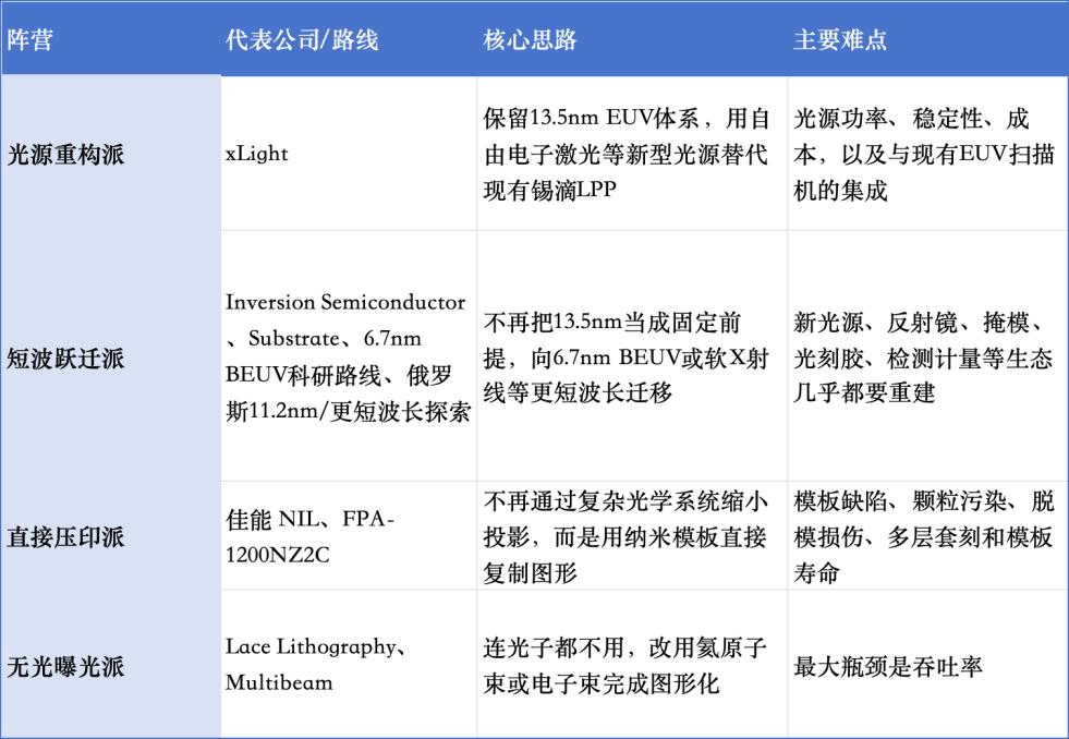
(Compiled and tabulated by Semiconductor Industry Watch)
(1) Light Source Reconstruction Camp
This camp is trying to change the generation method of 13.5nm EUV light, to solve the problems of insufficient power, high energy consumption and complex maintenance of the existing laser-produced plasma light source.
The representative enterprise is the US startup xLight. At present, ASML's EUV system mainly uses laser to bombard tin droplets to generate plasma, and then release 13.5nm EUV light. xLight hopes to replace the existing laser-produced plasma light source with a free electron laser, to centrally provide higher power and more stable light source for multiple EUV scanners.
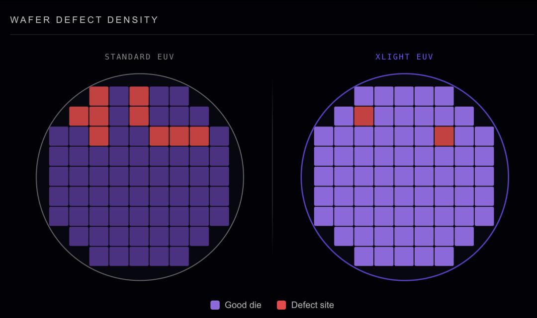
Defect distribution of traditional EUV and xLight EUV solutions on the same wafer (Source: xLight)
xLight mentioned on its official website that in a manufacturing system based on TSMC's 3nm wafer unit price of about 19,500 US dollars, the cost of traditional EUV equipment accounts for 40% of the total chip manufacturing cost; while the FEL (Free Electron Laser) EUV solution proposed by xLight can reduce the EUV-related cost by 50%, making its proportion in the total cost drop to 20%, thereby directly reducing the total manufacturing cost of the entire wafer by 20%.
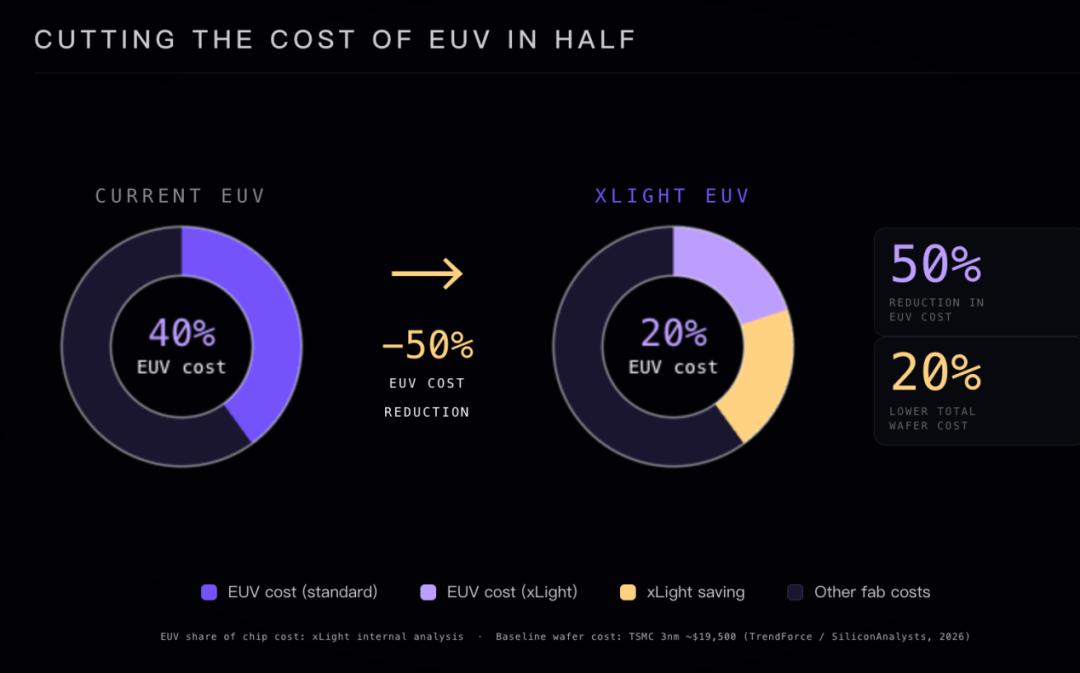
Cut EUV cost in half (Source: xLight)
(2) Short Wavelength Transition Camp
ASML's current EUV lithography machines, whether the 0.33 NA NXE or the 0.55 NA High-NA EXE, still use 13.5nm EUV light. The difference is that High-NA increases the numerical aperture from 0.33 to 0.55, further increasing the single exposure resolution to about 8nm, and continues to support 2nm and subsequent logic processes.
But another group of enterprises and research institutions began to think about a more radical question: Even if 13.5nm EUV can be continuously extended with the help of High-NA, it will still face a series of challenges in the