HardKrypton Exclusive Premiere | A veteran silicon photonics team has secured tens of millions of yuan in angel round financing, targeting next-generation CPO/OIO optical interconnection solutions.
36Kr Hardmolecule learned that Liangyin Technology, an optical chip enterprise, has recently completed a multi-million-yuan angel round of financing, led by Zhuhai Science and Technology Industry Group, with participation from Zhuhai Zhengfang Group and Shunwei Capital. The financing will be used to expand the team, iterate tape-outs and supplement equipment.
Founded in 2024, Liangyin Technology focuses on the field of photonic integrated circuits, and is committed to the R&D and application of silicon photonic transmission chips (PIC), Optical IO (OIO) and Co-packaged Optics (CPO).
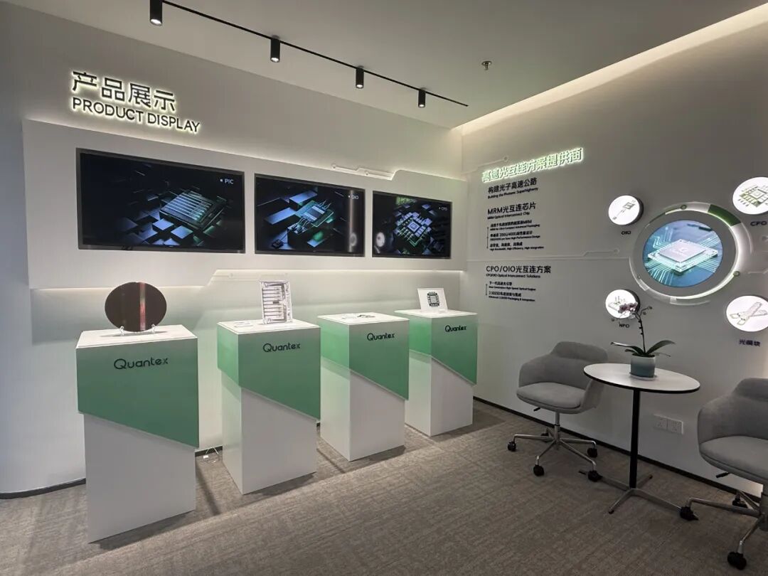
Source: the enterprise
The company's founding team integrates R&D and manufacturing experience from home and abroad. Founder Li Yaoji has more than 30 years of experience in the integrated circuit industry, and has served as Vice President of Engineering at Chongqing United Microelectronics Center (CUMEC), Chief Technology Officer of Cadence China, and Deputy Director of the Hong Kong Branch of the National Special Integrated Circuit System Engineering Technology Research Center, with rich resources and technical accumulation in the semiconductor industry in both the United States and China.
Co-founder and CTO Zhao Jingxiong once served as Technical Director of CUMEC, and technical lead at Cisco USA and Intel, with years of experience in architecture design of AI GPU/NPU/Switch/silicon photonic chips. Chief Scientist Craig Peterson is General Manager of Intel's Microelectronics Center, who has worked at Intel for many years and participated in the design of three processors and eight generations of chipsets.
With the explosive growth of generative AI and large model training demands, the scale of computing power clusters is undergoing unprecedented exponential growth, and the transmission rate is moving towards 1.6T and even 3.2T. This means that traditional signal modulation methods are faced with high power consumption, concentrated heat flux density and high risk of physical link flicker disconnection, and the traditional electrical transmission network based on pluggable optical modules is hitting the physical ceiling. To bridge the gap between supply and demand, deeply integrating optical engines with computing chips or switch chips, that is, moving from the pluggable mode to CPO and even OIO, has become the industry-recognized only path to ultra-high-speed optical interconnection.
According to forecasts from LightCounting/Yole, CPO will first see explosive growth in the next few years, while OIO, which will eventually penetrate into every high-end GPU/CPU, implies a potential market of hundreds of billions of dollars. Liangyin Technology enters this high-threshold track by taking micro-ring modulators (also known as "MRM"), the core device of CPO and OIO, as the entry point.
Compared with traditional EML or MZM modulation schemes, MRM has an extremely small physical size at the micron level and a driving voltage as low as 1V, which can natively adapt to high-density advanced packaging and significantly reduce system energy consumption. On this basis, Liangyin Technology has built 1.6T and higher-rate silicon-based optical chips based on the self-developed 200G per-channel MRM.
At the same time, the company is working on the layout of CPO solutions that match the next-generation interconnection architecture and Optical I/O Chiplets products for chip-level interconnection. Its solution aims to greatly shorten the electrical transmission distance, remove high-power-consumption DSP chips, reduce the energy consumption of system optical interconnection to an extremely low level, and build a high-speed and low-energy-consumption optical transmission "highway" for ultra-large-scale data centers.
In response to the industrialization problem of temperature sensitivity that is common in MRM technology, Liangyin has self-developed real-time temperature control feedback and electrical equalization algorithm IP, which ensures the stable operation of micro-ring modulators in the harsh data center environment. More critically, the company has mastered the underlying self-development capability of silicon photonic PDK (Process Design Kit), and adopts a mature, domestically independent and controllable CMOS process node for production, avoiding the supply chain risk of high-end processes from the source.
The following is an excerpt of the interview with Zhao Jingxiong, CTO of Liangyin Technology:
Hardmolecule: The OIO track is very hot right now. What is Liangyin's core advantage over its peers?
Zhao Jingxiong: First of all, we have substantial tape-out and testing experience, rather than only staying at the simulation stage. The core of OIO is tight optoelectronic interconnection, and overseas giants such as NVIDIA, AMD and Ayar Labs all take the MRM (micro-ring modulator) route in computing and high bandwidth density applications. We have the experience of multiple design iterations in the past. The company's latest 1.6T MRM optical chip tape-out this year has been completed and is currently under testing, giving us a first-mover advantage in China.
Secondly, our micro-ring FSR (Free Spectral Range) is designed to be relatively wide. OIO applications require an extremely large number of channels, and DWDM (Dense Wavelength Division Multiplexing) is generally adopted, that is, multiple wavelengths are placed under a single waveguide. If the FSR of the micro-ring is not wide enough, crosstalk will occur when modulating the first wavelength, affecting adjacent channels, making it impossible to place too many micro-rings for simultaneous modulation.
Last but most importantly, we have the underlying self-development capability of key devices, rather than relying on the PDK of the foundry. In fact, few fabs can provide micro-ring PDK at present. If we need to adjust device performance for some specific applications in the future, we will not face the difficulty of adjustment like teams that rely on standard PDK.
Hardmolecule: By developing the internal design library independently, can the yield be guaranteed when negotiating with foundries?
Zhao Jingxiong: This really hits the core issue. For the standard PDK provided by the foundry, the design usually gives priority to yield, so the performance parameters given are relatively safe and conservative, which is difficult to meet customized needs. When targeting specific application scenarios and differentiated customer needs, we will pay more attention to whether the performance matches, and make targeted adjustments on the design.
Of course, for the yield, we will collect data through multiple iterative tape-outs, and gradually adjust and optimize the design based on the data. This is the inevitable running-in process from engineering verification to mass production.
Hardmolecule: What are your plans for subsequent chip tape-outs?
Zhao Jingxiong: In the past, our development was mainly focused on the single-channel 200G MRM device itself, and the optoelectronic integrated chip we produced this time is a full chip. We have successfully integrated all functional devices such as multiplexers, waveguides, optical splitters, and PDs, which gives us a systematic grasp of the entire chip design process and functional device combinations. Next, we will continue to carry out multiple rounds of tape-outs to ensure high yield and reliability of the final mass-produced products.
Hardmolecule: What is the biggest problem currently facing the establishment of a domestic optical interconnection ecosystem? What does Liangyin plan to do?
Zhao Jingxiong: Abroad, there is a closed ecosystem driven by computing and switching giants like NVIDIA. But in China, the industrial chain is not yet fully in place, and it still takes time for the three major sectors mainly involved in optical interconnection, namely computing chips, optical chips and advanced packaging, to form effective collaboration.
Facing the current situation, we will first focus on our main business, make good optical chips, and cooperate with upstream and downstream to ensure the stability of the supply chain of key devices such as Driver IC, TIA and lasers. In the direction of CPO/OIO, we have reached cooperation with leading domestic GPU manufacturers and entered the PoC stage, focusing on overcoming the optoelectronic signal conversion and protocol layer adaptation between the interface, GPU and optical engine. At the same time, we are simultaneously cooperating with packaging factories to carry out joint R&D of 3D stacking advanced packaging such as TSV.
Our positioning in the ecosystem is an enabler of core optical interconnection. We will take the lead in making domestic optical chips run smoothly in the new generation of computing power systems, and open up the imagination space for collaboration and development for the upstream and downstream of the industrial chain.