Panoramic Breakdown of AI PCB Industry Chain Investment
The global PCB output value will exceed $120 billion by 2030, with AI PCB surging at a 32.6% CAGR, 4 times the industry average.
From the 18-layer design of NVIDIA's H100 to the 78-layer configuration of Rubin Ultra, and onward to 100+ layers on the future Feynman platform, AI servers are elevating PCB from a simple "circuit carrier board" to semiconductor-grade precision manufacturing.
This article systematically breaks down the three transformative shifts AI brings to the PCB industry: non-linear jump in layer count, generational upgrade of copper-clad laminate materials, and mSAP process substitution, while mapping out investment opportunities and the industrial landscape across four key equipment segments: drilling, exposure, electroplating, and inspection.
01
PCB: The Mother of Electronics, AI Reshapes Growth Logic
PCB, or Printed Circuit Board, is the foundational platform for interconnecting electronic components, widely hailed as the "mother of electronic products".
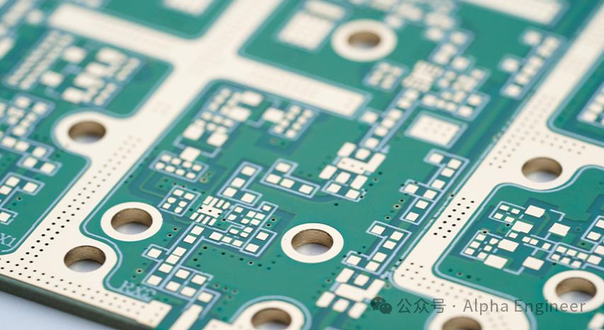
Figure: PCB Board
The PCB manufacturing process is analogous to constructing a "microscopic multi-story building".
First, copper foil (conductor layer), fiberglass fabric (insulating skeleton), and resin (bonding material) are fabricated into Copper Clad Laminate (CCL). Subsequent processes including drilling, electroplating, lamination, and etching ultimately form the multi-layer interconnected circuit substrate.
PCB complexity varies drastically across different application devices.
Mobile phone motherboards typically have 8-12 layers, PC graphics cards 10-16 layers, while AI server GPU module boards often feature 20-46 layers, with the unit value skyrocketing from hundreds of yuan to tens of thousands of yuan.
According to Prismark data, the global PCB output value reached $85.2 billion in 2025, is projected to hit $95.8 billion in 2026 (+12.5%), and will reach $123.4 billion by 2030, representing a 7.7% CAGR from 2025 to 2030.
Currently, AI is reshaping the growth dynamics of the PCB industry. The AI PCB market will grow from approximately $9.1 billion in 2025 to $37.2 billion by 2030 (32.6% CAGR), over 4 times the industry average growth rate.
We now conduct a detailed analysis of the three key transformations AI is driving in the PCB sector.
02
AI PCB Transformation 1: Non-Linear Jump in Layer Count
AI server PCBs are undergoing a non-linear increase in layer count, evolving from the mature process range of traditional servers toward semiconductor-grade precision manufacturing.
Traditional server PCBs typically feature 14-20 layers, using M4/M5 grade FR-4 materials, with signal rates limited to 25-56Gbps NRZ.
Entering the NVIDIA DGX H100 era, GPU computing boards jumped to 16-18 layers of 6th-order HDI, while the interconnected UBB boards reached 26-28 layers of PTH, with CCL materials upgraded to M4/M6 to support 112G PAM4 signal rates.
This marks the starting point of PCB's transformation from a "pure system carrier board" to a "high-speed interconnection core carrier".
For the Blackwell platform's GB200/GB300, computing boards further iterate to 20-22 layers of 6th to 8th-order HDI, adopting M7/M8 grade ultra-low-loss CCL to accommodate 112G PAM4 signals.
With the Rubin (VR200) platform launching in the second half of 2026, the layer count transition reaches a qualitative leap.
Computing boards are upgraded to 26 layers of 8th-order HDI, the SwitchTray unit reaches 32 layers of PTH, and a 44-layer Midplane backplane is introduced for the first time, fully adopting M8/M9 grade materials to support 224G PAM4.
Looking ahead to 2027's Rubin Ultra, the orthogonal backplane layer count will surge to 78 layers, utilizing a multi-stage lamination scheme paired with M9-grade CCL and HVLP-4/5 copper foil.
The future Feynman platform (circa 2028) is progressing toward 80+ layers and even 100+ layers, supported by M10-grade CCL and 448G PAM4 signal rates.
Each additional PCB layer requires manufacturers to invest extra copper-clad laminate and prepreg materials, while doubling the drilling operations and tightening lamination alignment precision to ≤25μm.
M9 materials have relatively high hardness, increasing drill bit consumption to 5-8 times that of traditional boards.
Higher layer counts not only linearly increase material usage, but also exponentially raise processing difficulty and yield thresholds.
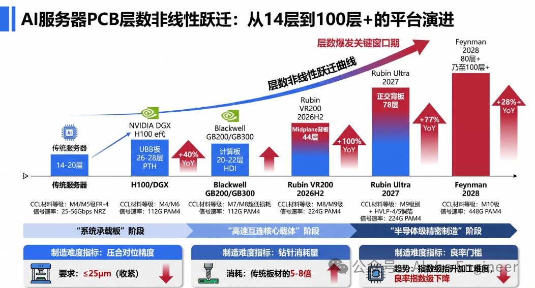
Figure: AI Drives Non-Linear Jump in PCB Layer Count, Generated by AlphaEngine
03
AI PCB Transformation 2: CCL Material Upgrade
As SerDes rates advance from 112G to 224G/1.6T, link insertion loss budgets are drastically compressed, forcing comprehensive upgrades to copper-clad laminates in Dk, Df, copper foil roughness, mechanical strength, and thickness uniformity. The material system migrates along the M7→M8→M8 path from low-loss to ultra-low-loss performance.
CCL materials evolve from M6 (Df≈0.002-0.003) → M7 (Df≈0.0015-0.002) → M8 (Df≈0.0010-0.0012) → M9 (Df<0.0007), with each generational upgrade bringing a 30-50% unit price increase, and M9 reaching 2.5-3.0 times the cost of M6.
This further drives synchronous upgrades across the three upstream raw materials of CCL.
- Copper Foil: Upgrading to HVLP4/5 ultra-low roughness (0.2μm), with the global market oligopolized by three players: Mitsui Metal, Luxembourg Copper Foil, and Taiwan's Jinyin. The HVLP copper foil supply-demand gap will reach 48% in 2026, creating strong upward price momentum.
- Fiberglass Fabric: Upgrading from standard E-glass fabric (¥8/m) to quartz Q-fabric (¥200/m), with Nittobo holding a dominant market position.
- Resin: Iterating from epoxy resin to hydrocarbon PPE/PTFE materials.
The 2025 global AI CCL market reached $2.2 billion (YoY +100%), with a projected $3.4 billion in 2026.
04
AI PCB Transformation 3: From Subtractive Process to mSAP
800G/1.6T optical modules require line widths reduced to 15μm and 10μm respectively. The traditional subtractive process has a physical limit of ≥50μm due to side etching effects, making a generational process shift inevitable.
To date, the industry has undergone three generations of process iteration:
- Subtractive Process: Etches away copper to form circuits, with mature technology but trapezoidal line cross-sections caused by side etching, limiting fine line precision;
- Additive Process: Selectively electroplates copper to grow circuits, offering high precision but weak bonding between copper layer and substrate, leading to insufficient reliability;
- Semi-Additive Process (SAP): Uses thin copper seed layer + pattern plating + flash etching, balancing precision and bonding force, but with complex chemical copper deposition processes and relatively high defect rates.
The current mainstream modified Semi-Additive Process (mSAP) for high-end substrates is an iterative improvement over the traditional SAP process.
mSAP replaces the chemical copper seed layer with a pre-fabricated ultra-thin copper foil substrate (RCC, 1–2μm copper thickness), eliminating one critical wet process. It delivers significantly lower process defect rates and better mass production stability than traditional SAP, enabling 15–25μm line width/space, near-rectangular sidewalls, and precision approaching IC packaging levels.
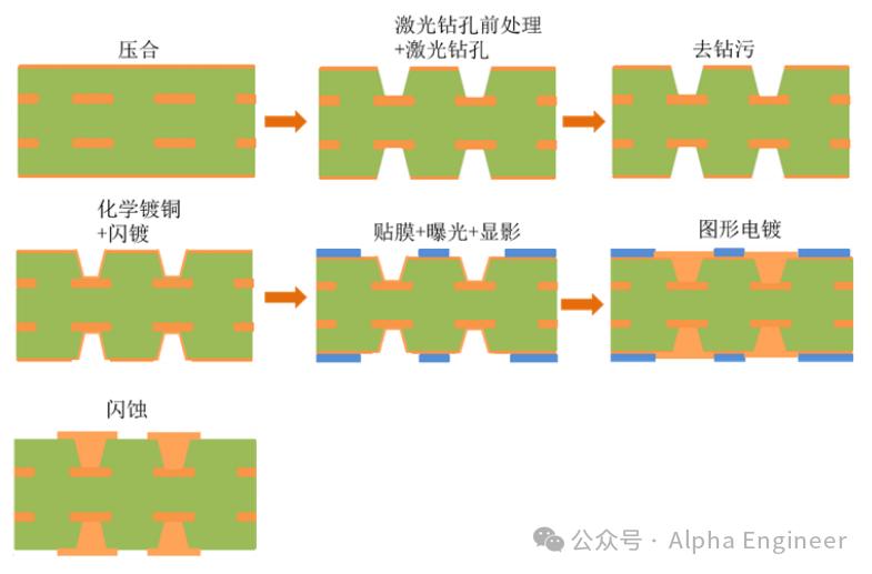
Figure: Schematic Diagram of mSAP Process
At the same time, mSAP improves material utilization from 50–60% in the subtractive process to 90%, though increased process complexity drives PCB unit prices 3–5 times higher, with gross margins jumping from 20–25% for traditional HDI to 40–50%+.
High-order HDI evolved from the (5+n+5) 6th-order design in the H100 era to the (6+14+6) 8th-order configuration on the Rubin platform, with exponentially increasing microvia density and processing precision, further raising process barriers and per-board value.
05
AI-Driven PCB-Specific Equipment Enters Structural Expansion Phase
The global PCB-specific equipment market is currently in an AI-driven structural expansion period.
According to Prismark data, the global PCB-specific equipment market size reached approximately $7.8 billion in 2025, projected to grow to $11.388 billion by 2029, with an 8.6% 2025-2029 CAGR significantly higher than the concurrent growth rate of global PCB output value.
The core logic behind equipment market growth outpacing PCB output growth lies in the "semiconductorization" trend of AI server PCBs (increased layer count, narrower line widths, material upgrades), which forces equipment technology iterations and drastically raises per-board equipment investment intensity.
Looking at equipment segment structure, drilling equipment accounts for the largest single share at ~21% (~$1.735 billion in 2025), exposure equipment and inspection equipment each account for ~15% (~$1.222 billion and ~$1.226 billion respectively), forming equipment 9% (~$700 million), electroplating equipment 7% (~$590 million), and lamination equipment 6% (~$476 million).
The top three segments combined represent over 50% of the equipment market, forming the core battlefield for equipment investment, which we analyze individually below.
06
PCB-Specific Equipment Investment Opportunity 1: Drilling Equipment
Drilling is the highest-value single segment in PCB equipment, and the process that benefits most significantly from AI server upgrades.
AI server PCB layer count jumps from 12-16 layers in standard servers to 24-40 layers, increasing total drill hole count by 20%-30%, while aperture shrinks from 0.25-0.30mm to ≤0.15mm. M8/M9 high-hardness materials reduce drill bit lifespan from ~3000 holes to 100-800 holes, requiring 3-5 sequential drill passes per hole instead of the traditional single pass, collectively driving drill bit consumption per AI server to 13.5-19.5 times that of a standard server.
Han's CNC (301200.SZ) is the global leader in PCB drilling equipment. In 2025, its drilling equipment segment generated ¥4.167 billion in revenue, up 98.38% YoY, accounting for 72.2% of total revenue.
Han's CNC holds ~50% global market share in ultra-high aspect ratio through-hole drilling machines, with AI-related revenue share projected to rise from ~30% in 2025 to 60% in 2026.
In the ultrafast laser drilling field, Han's CNC has begun batch shipments to SLP customers including AKM Meadville and Compeq. Mitsubishi's laser drilling equipment has a ~12-month delivery lead time, creating a significant window for domestic substitution.
07
PCB-Specific Equipment Investment Opportunity 2: Exposure Equipment
LDI (Laser Direct Imaging) exposure is the core equipment for PCB process upgrading in the AI era, with a global market size of approximately $1.222 billion.
The mSAP process requires line widths reduced to 15μm, demanding ±0.5μm imaging precision and ±1.5μm alignment precision from LDI systems, representing a 2-3 generational improvement over traditional exposure equipment.
AI server and 1.6T optical module PCB capacity expansion directly drives LDI demand, with the industry CAGR projected to exceed 15% during 2025-2027.
Orbotech (688630.SH) generated ¥1.408 billion in revenue in 2025, up 47.6% YoY, with attributable net profit of ¥290 million, up 80.4% YoY, and gross margins recovering to 40.2%.
With ~18% global market share, the company has surpassed Israel's Orbotech and Japan's ORC to become the world's largest manufacturer of PCB direct imaging equipment.
Its flagship MAS6P series LDI equipment achieves 6/6μm (line width/space) resolution, with production efficiency over 50% ahead of international comparable products, and has passed validation from leading customers including Unimicron and Shennan Circuits.
In Q1 2026, revenue reached ¥515 million, up 112.5% YoY, with net profit of ¥108 million, up 109% YoY, demonstrating a clear accelerating growth trend.
08
PCB-Specific Equipment Investment Opportunity 3: Electroplating Equipment
The global electroplating equipment market size is approximately $590 million, serving as a critical supporting segment for the mSAP process.
mSAP requires copper thickness uniformity controlled within ±5% (compared to ±10% for traditional processes), imposing stricter requirements on electroplating precision.
VCP (Vertical Continuous Plating) is the mainstream equipment for high-layer-count AI server PCBs, while horizontal 3-in-1 electroplating (desmearing + electroless copper + flash copper plating) is the core equipment for the mSAP front-end seed layer process.
DVIC (688700.SH) is the absolute domestic leader in electroplating equipment, generating ¥1.098 billion in revenue in 2025, up 46.4% YoY, with attributable net profit of ¥121 million, up 74.6% YoY.
Its VCP equipment holds over 50% domestic market share, with cumulative shipments exceeding 1,200 units, supporting board thicknesses from 0.1mm to 8