Hard Krypton Exclusive | Ion beam equipment provider raises over 100 million yuan in financing, with its products already delivered in batches to leading clients in optical communications, nuclear fusion, and quantum computing sectors
36Kr learned that Zhongshan Broad Opto-Electronic Technology Co., Ltd. (hereinafter referred to as "Broad Opto-Electronic") has completed a Series B+ financing of over RMB 100 million. Investors in this round include Yida Capital, CITIC Securities Investment, Dawu Venture Capital, FriendTimes, N Control Fund, with IO Capital acting as the exclusive financial advisor.
The raised funds will be used to introduce high-end talents, develop new products, and accelerate investment in integrated solutions, market promotion, and production capacity construction for key industry sectors that are showing explosive growth trends.
Founded in 2016, Broad Opto-Electronic is a national-level "Specialized, Refined, Differential, Innovative" little giant enterprise. The company focuses on fully domestically developed, self-controllable ion sources and ion beam ultra-precision process equipment, and is the only enterprise in the industry that has mastered the full-chain core technologies covering core component ion sources, ion beam complete equipment, and application process solutions, with independent R&D and in-house manufacturing.
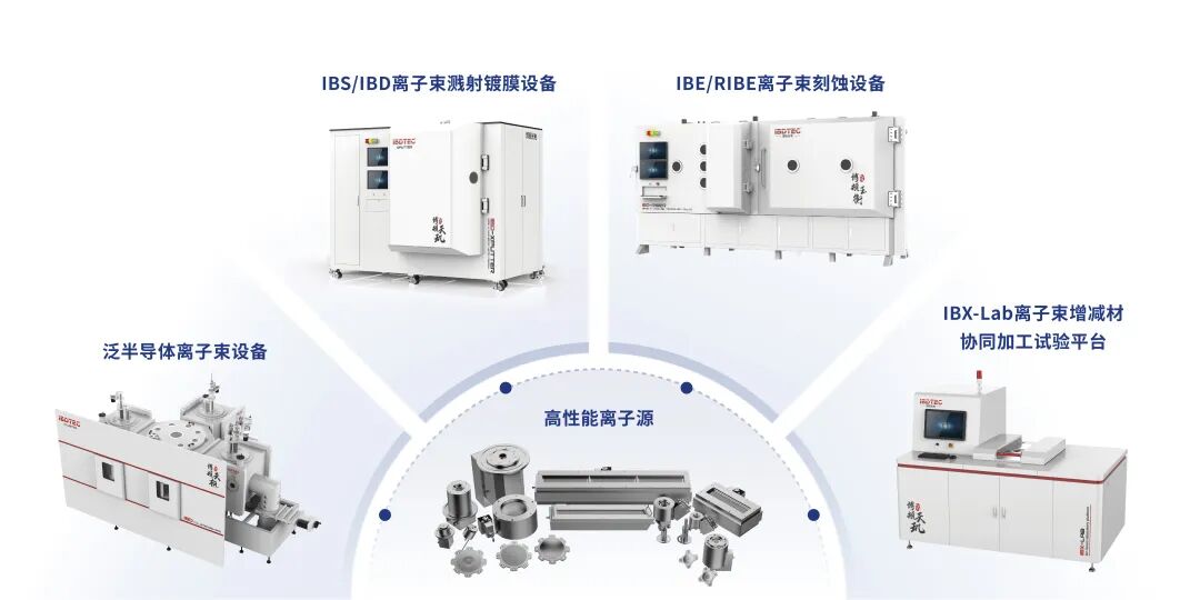
(Image source / the enterprise)
In terms of commercial implementation, Broad Opto-Electronic has built a solid performance base of stable cash flow from precision optics, general semiconductors, and aerospace. Meanwhile, with its rare market positioning, it has become the "exclusive shovel seller" of core process equipment for cutting-edge tracks such as controlled nuclear fusion, optical communications, and quantum technology. In recent years, the company's annual revenue growth rate has exceeded 50%.
For example, in the currently booming controlled nuclear fusion sector, Broad Opto-Electronic has demonstrated a dominant market share of nearly 100%. High-temperature superconducting tapes are irreplaceable materials for realizing high-field-strength magnets. In the preparation process of second-generation high-temperature superconducting tapes (REBCO system), using IBAD (Ion Beam Assisted Deposition) equipment to deposit the magnesium oxide seed layer is an unavoidable critical process. Broad Opto-Electronic is currently the only domestic manufacturer with the complete supply capability of IBAD ion sources and full sets of coating equipment for superconducting tapes, and has successfully entered the supply chain of almost all domestic high-temperature superconducting tape enterprises.
In the optical communication industry chain driven by the explosive demand for AI computing power, optical modules are rapidly evolving from 800G to 1.6T and even 3.2T. The demand for laser chips, modulation devices, detection devices in optical modules, as well as passive optical components such as narrowband filters and thin-film lithium niobate waveguides has surged sharply, and their performance parameters are forcing the rapid upgrading of technical architectures and processing techniques. Leveraging the process advantages of IBS/IBD in ultra-low thin-film loss, ultra-high precision of spectral parameters, and ultra-high resistance performance, as well as the differentiated capabilities of IBE/RIBE in high-precision etching of new compound materials like lithium niobate, the company has completed process introduction, order fulfillment, and equipment delivery for many leading enterprises in the optical communication sector.
In the quantum technology field, ultra-high-precision optoelectronic devices are the cornerstone of practical applications in quantum computing, quantum detection, and quantum communication. Traditional semiconductor processing equipment often fails to meet the requirements in terms of material system adaptability and extreme indicators. For example, under extreme parameters and process requirements such as atomic-level smoothness of components, ultra-low loss, ultra-low absorption, precise refractive index control, and special surface interface morphology treatment, ion beam thin film, etching, and shaping processes must be widely used. Broad Opto-Electronic has been approved for two major national quantum technology and instrument special projects as both a leading unit and a participating unit, empowering national-level scientific and technological task breakthroughs with fully independent ion beam core technologies and products.
The company's ability to rapidly enter leading enterprises in cutting-edge technologies stems from its ten years of deep technical cultivation. Ion beam is one of the most widely used micro-nano processing technologies, with processing accuracy reaching sub-nanometer and even atomic-level ultra-high precision. It features unrestricted material compatibility, diverse physical effects, wide energy range, high processing accuracy, and flexible manufacturing freedom, with applications covering thousands of industries and a market size of tens of billions of yuan. However, the technical and process application barriers for its development are extremely high, resulting in the domestic localization rate of high-end ion sources and ion beam equipment being less than 10% in the past, making breakthroughs in independent domestic development an urgent need.
With a number of domestically pioneering technologies and products, Broad Opto-Electronic has broken this "bottleneck" dilemma, realizing large-scale domestic substitution in multiple key fields.
Take the general semiconductor sector as an example: the company's high-performance ion sources have successfully achieved batch domestic substitution in segmented scenarios such as filter chips and various types of MEMS, and have passed the strict process verification and supplier qualification certification of leading foreign semiconductor equipment manufacturers, becoming the only domestic ion source manufacturer that has entered the semiconductor field and obtained continuous repurchases from customers.
At present, Broad Opto-Electronic is the ion beam equipment supplier with the highest domestic market share, the most product categories, the largest number of intellectual property rights, the widest range of application scenarios, and the most process application cases, and has full-chain commercial capabilities. In addition, Broad Opto-Electronic has been approved to undertake four national-level major science and technology special projects, and has taken on nearly 10 provincial and municipal science and technology plan projects, all of which have passed high-quality acceptance.
Ji Ming, founder of Broad Opto-Electronic, told 36Kr that the outside world used to have the impression that ion beam equipment had "extreme technologies and overly segmented application scenarios", considering it a narrow track with limited market capacity. However, the actual industrial development is the opposite. As the performance requirements of downstream cutting-edge industries approach the physical limit, the "atomic-level" ultra-high-precision ion beam processing method has gradually become the "only mandatory option". With the boom in industries such as commercial nuclear fusion and AI optical chips, the demand for ion beam processing equipment is rapidly being awakened and expanded.
The following is an excerpt from an interview with Ji Ming, founder of Broad Opto-Electronic:
36Kr: As the most critical component, what makes the technical barriers of ion sources so high? Why was it difficult for domestic players to develop high-quality ion sources in the past?
Ji Ming: Ion source technology is a highly systematic, multi-disciplinary integrated system. It seems to be a segmented field, but as downstream performance requirements rise, it has become a "necessary and irreplaceable" method in many scenarios, and the market size is growing very rapidly.
The difficulty lies in the deep cross-disciplinary coupling, including materials, mechanical structures, plasma physics, electronics and electrical control, software algorithms, and final application processes. Mathematics, physics, chemistry, mechanics, and software are all indispensable. As many foreign monopolistic companies in related fields often say: even if we put the drawings here, others may not be able to replicate the product, because there is a large amount of engineering know-how involved. For example, many components require special materials and special processing methods, including special power supplies and electrical control algorithms. All of these are independently explored by our team. Now we have delved deeper into the underlying ion beam simulation, combined with years of accumulated engineering experience, to support the independent R&D and in-house manufacturing of our full range of ion source products.
36Kr: Broad Opto-Electronic's product lines have in-depth coverage from precision optics, general semiconductors, nuclear fusion to quantum computing. What is the underlying development logic for Broad Opto-Electronic to enter these different industries?
Ji Ming: Focusing on ion beam ultra-precision equipment and processes is our unshakable main line. Vertically, we develop ion beam complete equipment based on fully self-developed ion sources, and extend to downstream applications to develop integrated process solutions. Horizontally, we continue to research and develop various categories of ion sources and ion beam ultra-precision equipment, fully covering process application scenarios such as coating, etching, and shaping, and iteratively launch new products following the evolution of downstream industry applications.
Ion beam equipment is a very common type of fundamental equipment. In the field of nano-level and even atomic-level ultra-precision processing, it acts like an "industrial machine tool" — a general-purpose processing equipment, so it covers a very wide range of industries. We do not blindly chase industry hotspots, but focus on perfecting common technologies and underlying products. Every industry has its own development cycle. When the cycle of a certain industry arrives, we will develop targeted products and solutions to adapt to the specific differences in application scenarios and process indicators of that industry.
36Kr: After this round of financing, what are the specific new plans for Broad Opto-Electronic in product development, R&D, and market expansion?
Ji Ming: Next, we will carry out planning in several main dimensions: At the ion source level, in the semiconductor sector, our ion sources have entered the supply chain of leading foreign complete equipment manufacturers, following the logic of replacing European and American products. In addition, we have accumulated a lot of technical reserves in fields such as advanced packaging bonding, and will launch new product categories. In the controlled nuclear fusion sector, we will continue to invest in the high-temperature superconducting tape field to maintain our absolute leading market share.
At the ion beam complete equipment level, for the ion beam thin film deposition product line, targeting sectors with surging demand such as optical communications and aerospace, we have already entered the supply chain of leading customers in various industries, and will subsequently increase the provision of process solutions and expand our product lines. For the ion beam etching product line, targeting sectors that are about to enter mass application in the next 2 to 3 years, such as optical communications and AR optical waveguides, we will continue to increase R&D and market investment.