Photons succeeding electrons: A computing revolution about to unfold in space

A bustling field crowded with brilliant minds often conceals hidden pitfalls. Staying patient and persevering in steady efforts, remaining undervalued and biding time in obscurity before reaping staggering returns, finds its latest example in NVIDIA.
In its early days, NVIDIA's CUDA, a peripheral team seen as "doing unproductive work," was tacitly allowed by Jensen Huang to operate without profitability for years on end, enduring sustained pressure, until Geoffrey Hinton, Ilya Sutskever, and Alex Krizhevsky invented the convolutional neural network AlexNet, which achieved legendary status at the 2012 ImageNet image recognition competition.
That year, the "Google Cat" (The Cat Neurons project) team used 16,000 CPUs but only achieved a 74.8% recognition accuracy. In stark contrast, AlexNet used just 4 NVIDIA GPUs to reach an astonishing 84% recognition accuracy, sending shockwaves through both academia and the industry.
The GPU, once a secondary component in gaming graphics cards, instantly became the core computing power driving the deep learning era. NVIDIA's market capitalization has since skyrocketed, surging from the tens of billions of dollars range to nearly 3 trillion dollars today.
Today, the very same narrative is quietly unfolding in another field.
Optical computing, a technological direction that lay dormant in laboratories for years, is now embracing its own "AlexNet moment" amid the voracious computing power demand of large model inference. From 2012 to the present, the GPU's succession to the CPU represented a computing power revolution for the deep learning training phase. Next, the succession of the GPU by optical computing will likely be the energy efficiency revolution for the large model inference phase.
Since the Transformer architecture emerged in 2017, the parameter count of large models has expanded from hundreds of millions to trillions, and every Token generated during inference requires massive matrix multiplication operations. Optical computing, by coincidence, possesses inherent advantages in both matrix multiplication and low power consumption. It is not a simple upgrade to electronic computing, but a fundamental restructuring of the computing paradigm — replacing electrons with photons, replacing electron drift velocity with the speed of light, and replacing serial switching with optical field parallelism. It has been verified to deliver 8-fold, 100-fold, or even 1000-fold speed improvements in AI matrix computing.
The integration of optical waveguides and semiconductor processes "simulates" large-scale AI matrix computing through purely physical means, which is incredibly fascinating. The history of technological development never repeats itself. When the old computing paradigm approaches its physical limits, new paradigms will emerge from the fringes, until the day demand explodes and they become mainstream.
That day for optical computing may be arriving right now.
In the AI Era, Electronic Computing Is Not "AI Native"

Image sourced from the official Lightmatter website
In 2017, a paper published in Nature Photonics also caused a stir within a small professional circle.
In this later widely cited paper, Nicholas Harris, founder of Lightmatter, verified a critical hypothesis: using photons to perform matrix computing is feasible. The core contribution of this paper, themed "Deep Learning with Nanophotonic Circuits," was not to immediately deliver commercial products, but to advance "photonic computing" from a conceptual idea to a verifiable engineering roadmap for the first time.
This roadmap included two layers of verification: first, at the hardware level, optical interference networks could handle programmable matrix operations; second, at the algorithm level, the neural network computing process could be restructured around the characteristics of optical hardware to minimize components unsuitable for optical computing.
Why is optical computing inherently suited for AI?
The core operation of deep learning, matrix multiplication y = Wx, essentially means each output component is the sum of input components weighted by their respective coefficients. In electronic chips, this requires continuous movement and accumulation of numerical values through individual switches; but in optical paths, the input vector is encoded into the amplitude and phase of the optical field in each waveguide. These optical fields are redistributed according to weights through a network of Mach-Zehnder Interferometers (MZIs), and finally the "summation" is completed via interference and detection at the output end.
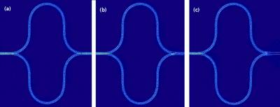
The image shows the MZI demonstration on the official Lightmatter website
A standard MZI consists of two 50:50 beam splitters and phase modulators in its two middle arms, essentially acting as an adjustable 2x2 linear transformation unit. A single MZI can only perform low-dimensional transformations, but cascading many MZIs in a specific topology can form a high-dimensional matrix network.
In real optical computing operations, assuming there are 4 input optical signals and the goal is to perform a 4x4 linear transformation, the approach is to feed the 4 optical paths into a grid composed of multiple MZIs. Each MZI is adjusted to a specific coupling ratio, and after several stages, the light intensity at the 4 output ports corresponds to the result of the matrix multiplication.
Optical networks do not perform term-by-term numerical calculations, but naturally complete the linear algebra calculation process using wave superposition.
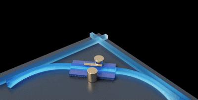
The image shows a demonstration of large-scale AI matrix computing on an optical chip from China-based Optical Base Technology
The advantages of optical computing are intuitive and clear: ultra-low latency due to the extremely fast propagation speed of light; low power consumption, as it does not require massive charge movement and switch toggling like electronic chips; and inherent compatibility with matrix multiplication, especially suitable for large-scale linear operations.
However, to bring these advantages from laboratories to the real world, different companies have chosen different technical paths. The two representatives are Lightmatter in the United States and Optical Base Technology in China — Lightmatter is the representative of the MZI route, while Optical Base Technology follows the photonic in-memory computing path.
Lightmatter chose the MZI route. The advantage of MZIs lies in their reconfigurability: the phase and amplitude of optical signals can be precisely regulated through thermo-optic or electro-optic effects, cascaded to form complex interference networks, and realize arbitrary unitary matrix mapping. This architecture is suitable for building programmable, high-precision optical neural networks and linear operation units.
Lightmatter's core product, Passage, is the world's first 3D-stacked silicon photonic engine, capable of delivering unprecedented bandwidth density and energy efficiency for XPUs (such as GPUs and TPUs) and switches.
In 2026, Lightmatter launched the Passage L20 optical engine, a 6.4 Tb/s 3D-stacked optical engine scheduled for mass production in the second half of 2026. In addition, Lightmatter plans to launch the L200 series, manufactured by GlobalFoundries and Amkor, using GF Fotonix silicon photonic platforms to integrate photonic components and CMOS logic onto a single die.
However, the problem with the MZI route is: it relies on thermal tuning, feedback calibration, and temperature compensation to maintain stable optical states, which means continuous power consumption and control overhead. The volatile tuning methods of traditional silicon optical waveguide devices require continuous power supply to maintain optical states, resulting in issues such as high static power consumption, large weight unit size, and low computing power density, which severely restrict the scalability of optical computing networks.
Optical Base Technology from China has pioneered an alternative path.
In 2022, two young men under 30, Xiong Yinjiang and Chen Tangsheng, made a series of decisions that seemed nearly crazy to outsiders, much like many familiar entrepreneurial stories. Xiong Yinjiang shut down his company in the United States, Chen Tangsheng paused his doctoral studies at the University of Oxford, and the two returned to China at a critical juncture to found the company "Optical Base".

Image sourced from public interview footage
Xiong Yinjiang holds a master's degree from the University of Chicago, with years of hands-on engineering experience in large model algorithms and AI Agents. Chen Tangsheng once studied under Harish Bhaskaran, the world's leading expert in "phase change material optical computing" and a Fellow of the Royal Academy of Engineering.
The motivation driving them to start their business was that they both foresaw an approaching inflection point: the explosion of AI demand is imminent, and optical computing chips may truly break through Moore's Law and solve the computing power anxiety.
In a recent public interview, Xiong Yinjiang and Chen Tangsheng shared a thought-provoking statement: "We particularly dislike working in fields crowded with people. We naturally tend to see those places as potential traps. When something is at its peak of popularity, we dare not engage in it. On the contrary, when we possess certain advantages that only we are aware of, before the field has fully taken off or exploded, that is the right time to devote our efforts to it."
This judgment of timing runs through the entire development process of Optical Base.
In 2017, although the landmark foundational paper on optical computing attracted attention, at that time, industry chain links such as Fab manufacturing and packaging processes at home and abroad were not yet mature, making commercial implementation difficult to advance. By 2022, the explosion of AI and the gradual maturity of the overall industry chain created the perfect opportunity for design companies to step forward, proactively drive the accelerated iteration of the industry chain through demand traction, which is exactly when Optical Base chose to enter the market.
Looking across the industry, most optical computing solutions still fall short of the standards for truly large-scale, universal, and stable deployment compared to electronic computing.
The two most prominent problems are: first, storage and computing are still separated. During AI inference, model parameters need to be frequently moved from external storage to computing units, making storage bandwidth the bottleneck of the entire system; second, large-scale integration is difficult. Constrained by the physical limitations of silicon photonic platforms in chip size, warpage deformation, and interconnection density, traditional optical computing solutions cannot easily expand their computing power scale.
Optical Base Technology's breakthroughs are precisely targeted at overcoming these two barriers.
Optical Base Technology is currently the only company in the world that has simultaneously realized photonic in-memory computing and glass-based optical computing. Photonic in-memory computing delivers tremendous benefits for AI inference: large model parameters can be stored directly inside the chip, completely eliminating the frequent data movement between storage and computing, reducing computing latency to one-tenth of that of traditional optical computing solutions.
Based on the in-memory computing technical route, Optical Base Technology has developed the optical computing chip with the world's highest computing power density. This chip has undergone multiple tape-out verifications and is ready for "out-of-the-box use", becoming a product-level application that truly connects the entire industry chain and the front and back ends of computing. Optical Base launched its first-generation optoelectronic fusion computing card in 2025, with the second generation scheduled for release in 2026.
Building on existing foundations, Optical Base is also advancing a more disruptive technical path: replacing silicon with glass as the substrate for optical computing chips, using glass simultaneously as the optical path carrier, packaging base, and large-scale manufacturable platform. This model creates a more scalable base platform natively designed for large-scale optical interconnection and optical computing, fundamentally breaking through the limitations of silicon photonic platforms in size, warpage, and interconnection.
Compared with the conventional pace of technology companies, Optical Base's productization progress is astonishingly fast. After the company was founded, it rapidly completed iterations of matrix scales such as 16×16 and 25×25, and achieved tape-out of a 64×64 matrix scale in 2023. In June 2024, Optical Base completed the world's first tape-out of an optical computing chip whose computing power density and computing power precision reached commercial standards, with a 128×128 matrix scale, breaking the industry's 3-year-old matrix size ceiling of 64×64.
In 2025, Optical Base's first-generation optoelectronic fusion computing card, based on the 128×128 optical computing chip, secured large orders from vertical large model companies, and completed the deployment of large models in the financial field — marking the world's first implementation of similar computing cards in large model scenarios.
Lightmatter and Optical Base represent two optical computing routes and two future outlooks. Lightmatter pursues "reconfigurable, programmable, flexible and universal AI computing", while Optical Base pursues "lower power consumption and dedicated AI inference with integrated processing and storage". In a specific scenario, Optical Base further amplifies its advantages of efficient, low-power AI inference computing — that scenario is space.
Bringing AI Computing Power to Space: Optical Computing "Succeeds" the GPU in Orbit
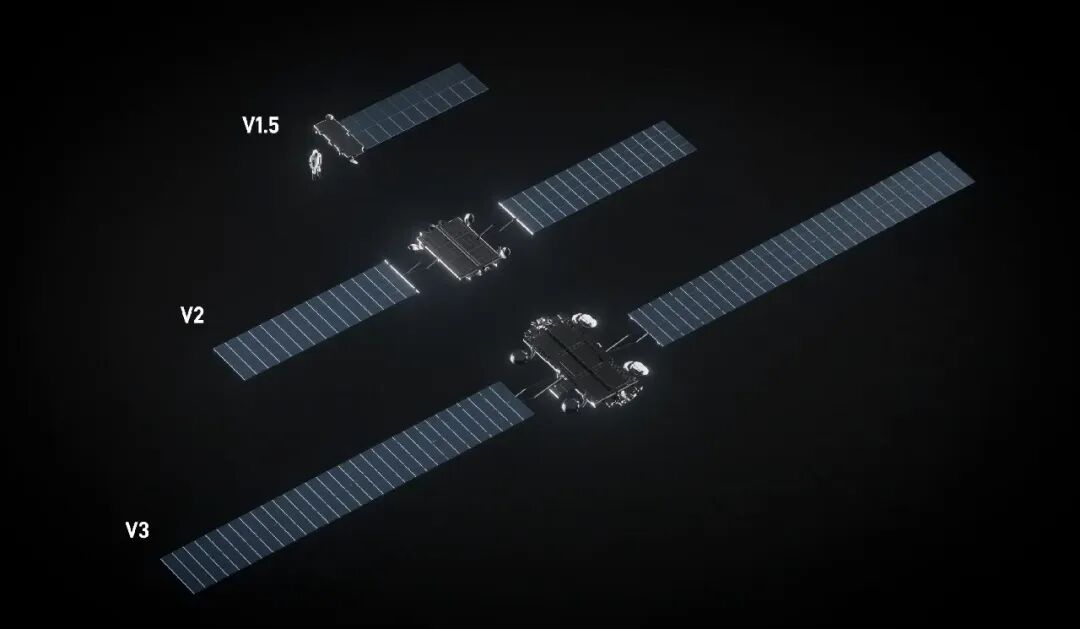
On June 12, 2026, SpaceX officially listed on the NASDAQ. With an offering price of $135 and fundraising of $750 billion, it shattered the global IPO historical record, surpassing Saudi Aramco's $294 billion fundraising in 2019, corresponding to a valuation of approximately $1.77 trillion.
The market is paying for a highly expansive narrative.
SpaceX plans to deploy up to 1 million AI computing satellites. Elon Musk's prediction is extremely ambitious: achieving an annual deployment rate of 1 gigawatt (GW) of space AI computing power by the end of 2027, seeking to expand by orders of magnitude every year, and eventually reaching a computing power scale of 1 terawatt (TW). 1 gigawatt is roughly equivalent to the capacity of a large nuclear reactor unit. At 1 terawatt — the AI computing power in space will exceed the total on Earth.
NVIDIA is also bullish on "bringing computing power to space". At the 2026 GTC conference, Jensen Huang announced the launch of the Space-1 Vera Rubin module, a product specifically designed for orbital data centers. Compared to the H100 GPU, the Rubin GPU in this module delivers up to 25x improvement in AI computing power for space-based inference. Jensen Huang stated at the launch event: "Space computing, this final frontier, has arrived. Wherever data is generated, intelligence must be present."
Why space? Elon Musk ran a clear-headed calculation, focusing on chips, storage, and energy. Space can efficiently and around the clock absorb sunlight and convert it into electricity, meaning "unlimited energy" with near-zero electricity costs. The space