Why has this century-old monosodium glutamate enterprise provided indispensable key materials for AI chips?
In recent years, AI chips have essentially become the barometer of the capital market.
Every new chip launched on the market immediately draws widespread attention from all parties.
Yet few people know that a critical material called ABF Film is used in the packaging of many high-performance chips.
Without this film, the high-density circuitry inside the chip would be nearly impossible to lay out stably, and signals would struggle to transmit smoothly.
Surprisingly, the company that produces this material is Japan's Ajinomoto — a condiment manufacturer that started its business with monosodium glutamate.
Yet Ajinomoto has long supplied ABF Film for high-performance CPUs and GPUs, holding an almost unrivaled position in this niche market.
How did a company that made its name selling MSG become such a vital link in the AI chip supply chain?
The story begins with a bowl of kelp soup.
1
The Condiment Factory Born From a Bowl of Kelp Soup
In 1908, Kikunae Ikeda, a professor at Tokyo Imperial University, noticed that the kelp and cucumber soup his wife made for dinner tasted exceptionally savory.
As a chemist, he was curious about why kelp could enhance umami flavor, and decided to figure out exactly where that savory taste came from.
Through repeated experiments, he finally identified the source of umami in kelp: a substance called glutamic acid.
Later, glutamic acid was processed into its sodium salt — the familiar monosodium glutamate (MSG).
When he dissolved tiny crystals of this substance in clear water, the previously bland liquid instantly became savory, confirming his hypothesis: this was the source of umami.
However, a laboratory discovery does not automatically turn into a marketable product.
Well aware of his own shortcomings in business, Kikunae Ikeda sold the patent to a merchant named Saburosuke Suzuki.
Suzuki immediately recognized the huge business opportunity, named the product "Ajinomoto," quickly brought it to market, and achieved great success.
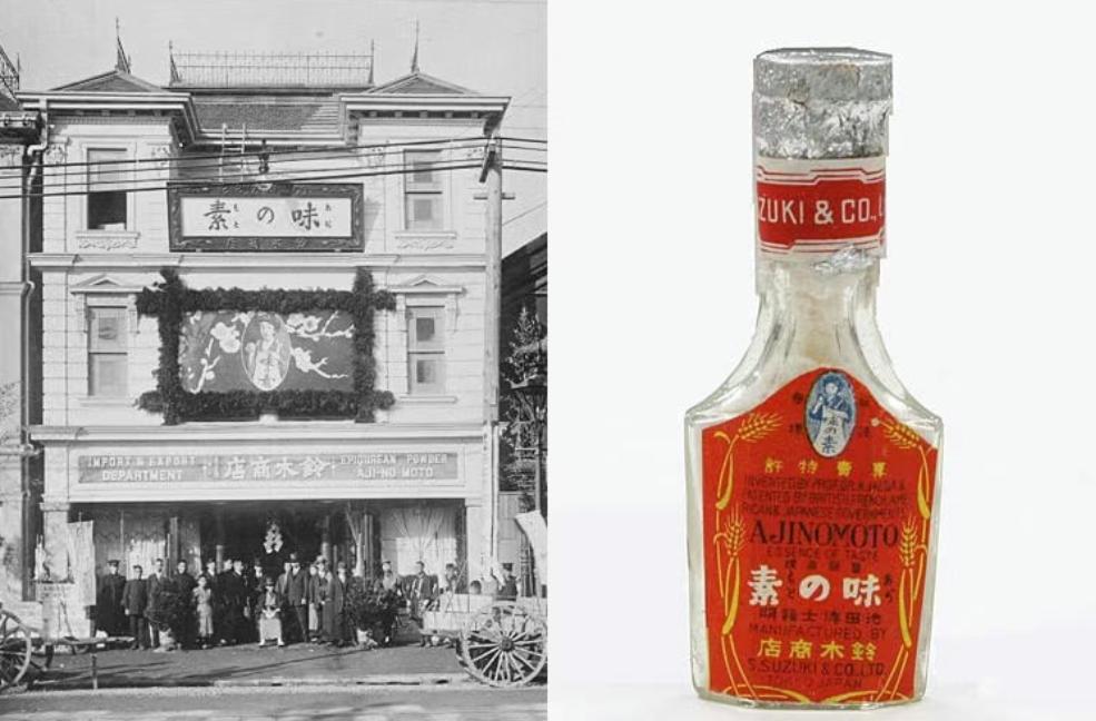
A scientist identified the source of umami from kelp, a merchant bought the patent, and a future world-famous condiment company was born.
This is roughly the standard opening for many legendary brands.
But if the story had ended there, it would be hard to explain why Ajinomoto later became an indispensable part of the global AI chip supply chain.
Because the real challenge was not finding umami in kelp — it was how to produce that umami consistently as a commercial product.
The umami in a bowl of soup can be tasted by humans, but how can manufacturers ensure consistent quality across mass-produced MSG?
A batch of MSG with inconsistent flavor might simply taste bad to consumers, but for producers, it represents a quality incident that seriously damages brand reputation.
The problem was that the purity of raw materials arriving each day was never perfectly uniform, and subsequent processes like fermentation and purification were affected by factors such as temperature and operational skill — making it easy for quality to vary slightly from batch to batch.
This meant that during production, the factory had to extract crystals with consistent purity, color, and flavor from impurity-filled fermentation broth.
To achieve this goal, Ajinomoto was forced to develop an extremely rigorous set of industrial control capabilities from the very first day of its founding — capabilities that it maintains to this day.
Consumers only see a small pile of white crystals, but the process expertise Ajinomoto built behind the scenes goes far beyond that.
It includes experience handling complex raw materials, precise control over formulas and impurities, and the persistence required to turn unstable materials into mature, reliable products.
Ajinomoto soon applied this expertise to amino acid production.
At that time, in the aftermath of World War II, Japan faced severe material shortages, and many people lacked sufficient protein in their diets.
Scientists soon discovered that simply supplementing protein was not enough — the human body also needs several essential amino acids that it cannot synthesize on its own.
On top of that, hospitals needed amino acid preparations to support post-surgery patients and those suffering from malnutrition; feed mills also began paying attention to amino acids, hoping to help livestock absorb protein more efficiently and grow faster.
Ajinomoto quickly realized that although it had long produced sodium glutamate, its accumulated expertise in fermentation, separation, and purification could easily be adapted to mass-produce other amino acids.
Leveraging its existing process foundation, Ajinomoto tried new fermentation and synthesis methods, successfully manufactured a wider range of amino acids, and began supplying to various customers with different needs.
From that point on, Ajinomoto's business gradually expanded from condiments into food, pharmaceuticals, animal feed, and fine chemicals — evolving far beyond being just a condiment company.
It was during this R&D process that Ajinomoto began experimenting with various chemical materials, testing them in relevant industrial scenarios to explore potential commercial applications.
2
A Material Line That Received No Applause
In the 1970s, Ajinomoto encountered several resin-like materials during condiment production and related chemical research.
These materials were not edible, nor could they be bottled and sold to consumers like condiments. From a traditional business perspective, these materials, which had no obvious use cases at the time, seemed like useless byproducts of research.
Yet this material, first discovered in the lab, would eventually become ABF (Ajinomoto Build-up Film) — the prototype of the product that would later find its way deep into the global high-performance chip supply chain.
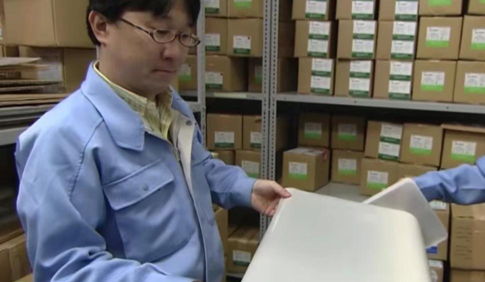
Through repeated experiments, Ajinomoto found that after processing, this type of resin material could form a relatively stable thin film with excellent insulating properties.
The problem was that few companies at the time showed any interest.
In that era, personal computers were not yet widespread, consumer electronics were just emerging, and chip packaging was nowhere near as complex as it is today.
The entire market had no incentive to seek out a brand-new insulating film. Even if lab data looked promising, it could not immediately translate into profitable orders.
Faced with this situation, most companies would have shelved the project and waited for market demand to emerge.
But Ajinomoto did not do that.
This was not because it could foresee the future of the semiconductor industry, but because this new material, once fully mature, could genuinely find a place in the electronic materials sector.
This kind of research was different from condiment development, which could quickly produce products that consumers could perceive. Most of the time, researchers were stuck in the lab, tediously adjusting formulas, processing methods, and material properties over and over again.
During the research process, problems kept popping up one after another.
For example: how to proportion the resin components? How to precisely control the thickness of the film? Could it cure stably after heating? Would it become brittle after curing? Would its insulating performance drift significantly in different temperature and humidity environments...
Each of these variables meant countless rounds of redoing the work from scratch.
As a result, Ajinomoto could only keep adjusting formulas and processes while quietly building a patent portfolio around potential application scenarios.
Although these patents seemed to have little commercial value at the time, they at least provided technical reserves to keep the material line moving forward.
While conducting intensive R&D, Ajinomoto also tried to launch this new material on a small scale, using it on ordinary circuit boards with less stringent requirements to verify its practicality.
While using insulating materials for circuit boards made perfect theoretical sense, the market was not yet urgent enough to immediately phase out older-generation products.
After all, for relevant manufacturers, old products still had a market. Abruptly switching to a brand-new insulating material would require revalidation and process adjustments — leading to a sharp cost increase that might not be cost-effective.
As a result, this material research and development fell into an awkward situation: it worked well in practice, but market demand was low, and the industry was far from reaching a point where it "could not do without it."
This meant that for a long time, this material line was trapped in labs, patent documents, and small-scale trials, quietly waiting for its era to arrive.
Interestingly, the outside world was almost completely unaware of this.
Even though Ajinomoto had been working in industries like amino acids, pharmaceutical raw materials, animal feed, and fine chemicals for years, most people still saw it as a company that only made MSG, condiments, and food products.
This material line long remained in an awkward "idle" state within Ajinomoto. It was not affiliated with any profit-making department, had no independent KPI assessments, and functioned more like a "technical outpost" that was granted special permission to exist.
Every once in a while, the team would take improved samples to electronics manufacturers to test the waters. Most of the time they were rejected, and occasionally they received small trial orders — just enough to keep the production line running, but far from enough to support an entire R&D team.
Ajinomoto did consider cutting the project.
At the peak of Japan's economic bubble in the 1980s, there were fierce internal debates: since condiment and amino acid businesses were highly profitable, why keep pouring money into a bottomless pit with no visible market?
But in the end, what saved ABF was not some far-sighted individual decision, but Ajinomoto's long-standing technical reserve mechanism: any direction related to the core business and covered by patent filings was allowed to continue operating at minimal cost, even if it ran at a short-term loss.
ABF perfectly met these criteria — it shared the fermentation and purification processes, and had a solid patent wall. Cutting it would mean losing all prior investment, while keeping it only required very low maintenance costs.
And so, the ABF R&D team did not expand, but also did not shrink. They continued day after day, adjusting formulas and recording data.
It was not until the early 1990s, when the global PC industry exploded, that a turning point arrived.
3
Catching the Wave of Industry Boom
At that time, the entire semiconductor industry was advancing under the momentum of the famous "Moore's Law." This law required continuous improvements in chip performance, which meant engineers had to cram more transistors into the same chip area.
This seemed like a technical goal, but in reality, it put enormous pressure on the entire industry.
As performance requirements rose, the number of transistors kept increasing, which meant circuits on the substrate had to be drawn ever denser, and connection points made ever smaller.
This pushed the limits of packaging processes again and again, and old insulating materials kept failing under the strain — leaving the entire industry struggling to find an alternative solution.
The emergence of ABF perfectly filled this gap.
Technically speaking, ABF was not some uncopyable black technology — it was more like a custom-made solution tailored for the packaging upgrades of that era.
This process not only enabled laser drilling to create smooth micropores at the micrometer scale, but also supported direct copper plating, making circuit conduction more stable.
More critically, ABF's physical properties were highly compatible with chips. Its thermal expansion coefficient was close to that of silicon wafers, which meant it could maintain structural stability at high temperatures even when substrates were stacked into more than a dozen layers.
This high level of compatibility made ABF meet the core needs of industrial upgrading. After sample testing, process verification, and customer onboarding, it quickly gained entry into the supply chains of major chip manufacturers.
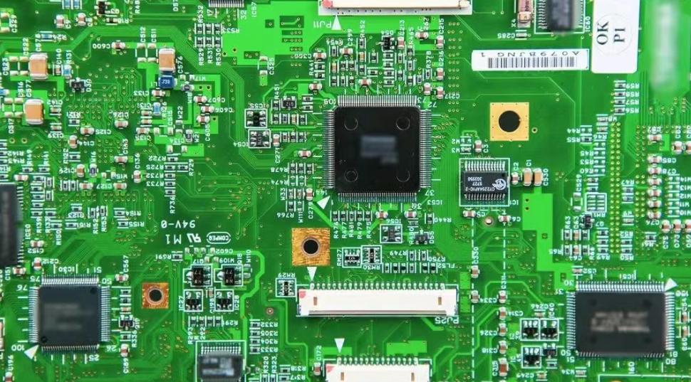
There were no shortcuts in this process — it relied on deep collaboration between the company and the entire industry chain.
To make ABF compatible with continuously evolving manufacturing processes, Ajinomoto's engineers were stationed on-site at packaging plants for years, working side by side with chip manufacturers' teams to debug equipment and adjust parameters.
At the same time, Ajinomoto kept iterating and optimizing ABF's formula to meet the packaging requirements of each new generation of chips.
This deep integration not only embedded ABF into the foundation of the industry chain, but also quietly transformed Ajinomoto from a food and chemical company into a critical supplier of chip infrastructure materials.
With the arrival of the AI large model era, demand for ABF has continued to grow.
The packaging complexity of GPUs and data center chips is an order of magnitude higher than in the PC era, with substrate layers, signal density, and power consumption all reaching unprecedented levels.
Driven by this trend, the electronic materials business has gradually become one of Ajinomoto's fastest-growing and highest-margin segments.
By the end of 2023, Ajinomoto's electronic materials-related revenue had exceeded 100 billion yen. Its share of the group's total revenue rose from single digits a few years earlier to nearly 10%, with a growth rate significantly higher than that of core segments like condiments and food.
In the following years, the electronic materials business remained Ajinomoto's highest-margin core growth engine.
ABF is no longer just "highly usable" — it has become a critical factor that ultimately determines whether chips can be delivered.
Given such high profits and the relatively uncomplicated ABF process, why haven't other manufacturers launched alternative products?
This is precisely why ABF is so hard to replace — this material has formed a highly coupled collaborative system with existing chip production lines.
Once ABF enters a production line, it is tightly integrated with the entire set of processes including laser drilling, copper electroplating, and lamination. It is like a core component of a precision instrument: replacing a single part often requires recalibrating the entire machine.
If you shut down the production line to replace ABF, you would have to readjust the power of laser drills, reset the plating solution ratio, and re-optimize the temperature and pressure of lamination.
This kind of comprehensive, disruptive adjustment would lead to massive losses and an extremely long adjustment cycle — a cost that chip manufacturers, who race against time, simply cannot afford.
Even if new competitors develop samples with similar performance, they still face extremely high entry barriers.
After all, the entire process — from sample testing to small-batch trial production, and finally to mass supply — takes at least one year, and as long as two or three years.
More importantly, besides the long R&D timeline, customers are more worried that unproven products might suffer yield fluctuations during full-scale production.
A more direct reason is the trade-off between cost and risk.
A high-end AI chip sells for thousands of dollars, while ABF accounts for only a tiny fraction of its total cost. No rational procurement decision-maker would risk yield drops and delivery delays just to save an insignificant amount on material costs.
Therefore, what Ajinomoto delivers is not just an ordinary insulating film — but a production collaboration system that has been verified over many years and cannot be easily replaced.
And this film has long been deeply embedded in the chip manufacturing process, making it almost impossible to separate.
4
The Next Card to Play in the AI Boom
In recent years, due to surging demand for packaging substrates from AI servers and high-end GPUs, ABF Film supplies have become tight, forcing Ajinomoto to continuously expand production capacity.
Ajinomoto has successively added new ABF Film production lines at its existing manufacturing bases in Gunma and Kawasaki, with the goal of increasing capacity by about 50% by 2030.
However, for Ajinomoto, expanding