TSMC places bulk orders, Cadence pursues serial acquisitions: Is the AI chip landscape on the verge of transformation?
Currently, AI chips and advanced manufacturing processes are continuously pushing toward extreme performance, causing many previously overlooked segments of the industrial chain to step into the spotlight one by one. Recently, a series of major moves on both the demand and supply sides of the EDA market have revealed that the competitive boundaries of AI chips are beginning to extend into fields such as PCB system interconnection, advanced packaging collaboration, and component data ecosystems.
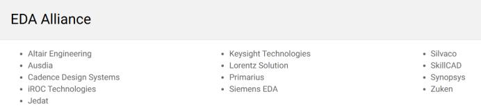
Let us first look at these two key developments: First, TSMC's new batch of EDA orders has for the first time added Zuken, a company specializing in PCB design and electrical system engineering, alongside the three major giants Cadence, Synopsys, and Siemens. Second, Cadence has successively acquired EMA Design Automation and FlowCAD to integrate their PCB design and component data capabilities into its electronic system design and analysis business ecosystem.
The former represents changes in market demand, while the latter reflects supplier capability integration. Both point to a more notable trend: the competitive boundaries of AI chips are extending beyond chip design and manufacturing to packaging, board-level interconnection, and even system-level collaboration.
01 The Shift in Demand Behind TSMC's First Introduction of Zuken
Since I started following TSMC's EDA ecosystem alliance, I have noticed that they update their supplier directory at least twice a year, and each update signals significant market shifts.
Not long ago, TSMC updated its EDA ecosystem again. In addition to further deepening cooperation with the three major EDA giants, it introduced Zuken for the first time. I believe this is not a simple expansion of the supplier list, but a further outward expansion of the boundaries of AI chip design.
Judging from TSMC's order distribution for the three major giants, Cadence focuses on advanced nodes such as N3, N2, A16, and A14, with core operations centered on AI chip-oriented design, including Design Technology Co-Optimization (DTCO), 3D-IC design, and design workflows for AI agents. Meanwhile, Synopsys has further strengthened its capabilities in 3DIC, CoWoS advanced packaging, multi-physics analysis, and Chiplet interconnection to support the high-bandwidth interconnection and complex packaging requirements of AI systems. Siemens EDA prioritizes AI-driven physical verification and automated repair, improving design efficiency for advanced nodes through multi-step automated DRC workflows.
It is not difficult to see that these services remain focused on the core chip design pipeline, while the addition of Zuken is distinctly different. Its core business covers PCB design, electrical system engineering, and board-level interconnection — all belonging to the system implementation layer outside of chips. This clearly shows that TSMC is no longer limited to chip design, and has begun to focus on how chips can be efficiently integrated into systems.
As is widely known, the production capacity of advanced packaging technologies like CoWoS remains tight, and whether chip performance advantages can be translated into system computing power increasingly depends on system-level collaboration capabilities after packaging. Therefore, TSMC's first purchase of Zuken's products indicates that the complexity of AI chips is continuously shifting from the chip design stage to the PCB and system interconnection layers.
02 Why Did Cadence Acquire EMA and FlowCAD?
The first collaboration between TSMC and Zuken is what drew my closer attention to Cadence's two acquisitions: EMA Design Automation and FlowCAD.
Beyond reinforcing its traditional PCB business, these acquisitions also significantly strengthen Cadence's core capabilities in electronic system design and analysis.
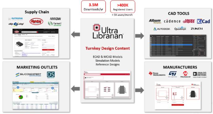
For example, EMA's key asset, the Ultra Librarian platform, provides a verified large-scale component database including schematic symbols, PCB footprints, 3D models, and supply chain data, supporting access across different CAD environments. Currently, the platform has over 400,000 registered global users.
This data demonstrates that component library management is no longer a secondary supporting segment. Especially as the complexity of AI servers, acceleration cards, and high-performance computing systems increases, component data has become a critical foundation affecting system design efficiency.
The underlying reason is easy to understand. Today's AI hardware complexity is no longer confined within chips — ultra-highly complex system-level integration is required between GPUs, HBM, high-speed SerDes, power modules, cooling systems, and high-speed connectors. As Cadence stated in its press release, for engineers and PCB designers, the ability to quickly access "accurate, production-ready component models" has become a key link that determines whether a product can move from concept to manufacturing.
It is reported that Cadence will deeply integrate EMA and FlowCAD's technologies into the Allegro X and OrCAD X platforms to enhance component library management, data validation, and collaborative design capabilities, helping engineering teams complete component search, validation, and integration faster. Therefore, in my personal view, Cadence's two acquisitions are not just for expanding PCB capabilities, but more importantly, for building a data infrastructure that extends from chip design to the entire system, allowing it to pre-position itself as the system-level design entry point in the AI era.
Combined with the earlier event of TSMC introducing Zuken, where demand-side players are enhancing board-level system design, EDA vendors are actively filling gaps in underlying data capabilities. Both developments fully show that the market focus is no longer limited to PCB tools, but on more complete system-level design capabilities.
03 What Trends Are Revealed in Financial Reports?
Financial data is the best proof. Cadence's backlog of orders hit a new record last quarter, reaching 8 billion U.S. dollars, confirming that "AI is continuously driving demand for complex chip and system design." Among its businesses, the IP segment saw a 22% year-on-year growth, driven by advanced node design, Chiplet architectures, and complex system applications such as AI, high-performance computing, and automotive electronics.
In addition, Cadence frequently references "Agentic AI" and "Physical AI." The former emphasizes using AI agents to drive design workflow automation, shifting EDA from a toolchain execution model to a goal-driven autonomous optimization paradigm. The latter refers to physical-level realistic simulation capabilities, enabling designs to more accurately map complex real-world constraints such as thermal, mechanical, and electrical characteristics.
"AI agents will run far more design experiments than human engineers, which will significantly increase the invocation frequency of underlying simulation and verification engines." Cadence's judgment reflects a disruption in design paradigms. With the widespread adoption of Agentic AI, the EDA business model will also shift to a hybrid "subscription + usage-based" pricing model, because the scarce resource in the future will no longer be software licenses, but high-precision simulation capabilities.
Such transformative changes are driven by a structural shift in design complexity. In the past, industry competition mainly revolved around transistor density, process nodes, and PPA optimization. Today, the bottlenecks that truly determine system performance largely lie outside the chip — cooling efficiency, power integrity, high-speed signal transmission, packaging stress, and board-level interconnection reliability, all of which have become new variables affecting AI computing power.
This is the fundamental reason why Cadence continues to strengthen system-level design capabilities: the market demands not just EDA tools, but proactive planning for complex system design paradigms.
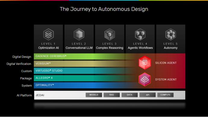
04 Building System-Level Design Infrastructure
For a long period in the past, PCBs were often regarded as a supporting segment in the semiconductor industrial chain, whose core values were limited to connection, component mounting, and routing, thus receiving far less market attention than advanced manufacturing processes, GPU architectures, or EDA software.
However, the AI era has redefined this positioning. With the accelerated adoption of GPUs, HBM, Chiplets, and advanced packaging, AI hardware is increasingly evolving into a highly complex system engineering. Whether chip performance can truly be converted into effective computing power no longer depends solely on the foundry's process capabilities, but also on the system implementation efficiency after packaging.
In a sense, advanced packaging solves the problem of bringing chips physically closer, while PCB and system interconnection address how these chips can collaborate more efficiently.
From TSMC's first introduction of Zuken to Cadence's reinforcement of PCB and component data capabilities through acquisitions, these seemingly separate events actually point in the same direction: Future AI hardware will not only focus on advanced processes and chip architectures, but also on packaging collaboration capabilities, system interconnection efficiency, and overall implementation speed.
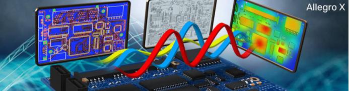
It is clear that Cadence is proactively positioning itself for the new design entry point in the AI era. Because the future value of EDA may not only lie in helping customers complete chip design, but more importantly, in connecting the entire closed loop from chips and packaging to system implementation. This may be the most notable change behind these two events: the definition of AI chips is evolving — it is no longer limited to the maximum computing power of a single chip, but rather who can more efficiently complete the entire design closed loop spanning chips, packaging, and system implementation.
This article originates from the WeChat Official Account "Kun Shao Says", authored by Kun Shao, and is republished by 36Kr with authorization.