The glass substrate suddenly accelerates
The market for AI computing power has advanced in waves. After one sector rises, another follows. Now, it's the turn of glass substrates.
In late May, BOE announced that it had signed a cooperation memorandum with Corning regarding glass substrates, completely igniting the market.
Not only did BOE's previously stable stock price skyrocket vertically, hitting the daily limit for two consecutive trading days, but also upstream companies such as Irisohyaku Co., Ltd. and Wufang Optoelectronics Co., Ltd. had their stocks hit the daily limit. The stock price of Dier Laser Co., Ltd. reached a record high, and the stock price of Vog Optoelectronics Co., Ltd. has soared threefold in the past two months.
Institutions have identified 2026 as the first year for the commercial verification of glass substrates. In addition to the cooperation between BOE and Corning, Intel announced the successful mass - production of glass core substrates for its latest server CPUs, and TSMC revealed the establishment of a trial production line for glass substrate CoPoS packaging.
These two giants are working hard, and the atmosphere for a significant price increase is well - set.
It has to be said that the commercialization speed of glass substrates has exceeded the expectations of most people.
Replacing the "Board" in Chips
Intel and TSMC are the leading proponents of glass substrates at present, but the "glass substrates" they refer to are not exactly the same.
A chip is composed of various components. These components are fixed on a carrier board to form a functional unit. These functional units are then fixed on the next - layer carrier board to form a larger functional unit, and so on, presenting a hierarchical structure.
For example, the circuit board we are most familiar with is the bottom - layer carrier board. If we disassemble it further, there are also core substrates, IC carrier boards, etc.
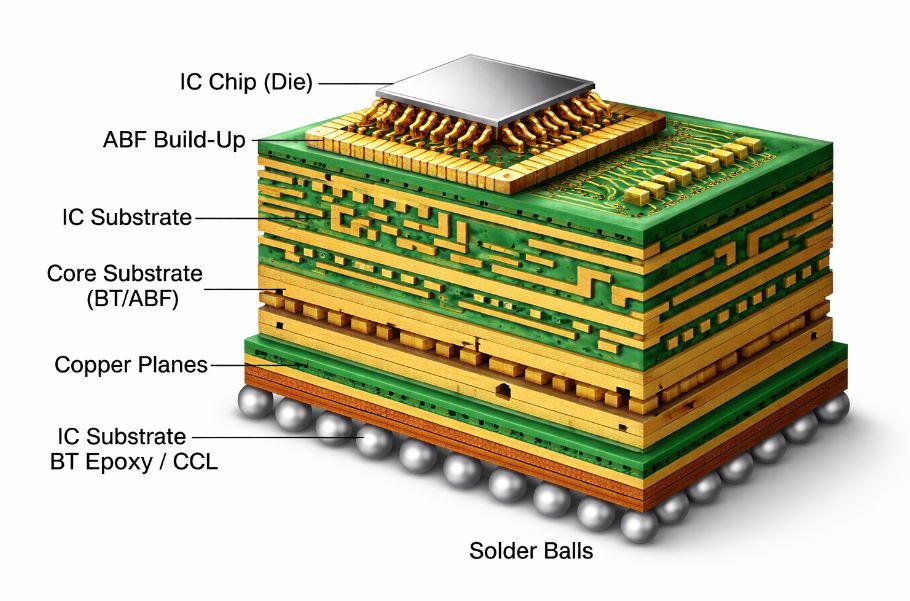
The "boards" at different levels inside a chip; Image source: IC Components
In the past, most of these carrier boards were made of materials such as resin, glass fiber, copper foil, and silicon. As the name suggests, a glass substrate is a substrate mainly made of glass.
What Intel and TSMC want to do is to replace the mainstream carrier boards with glass substrates, but they are not replacing the same "board".
Intel's "Advanced Packaging Glass Substrate", full - name "Glass Core Substrate", is intended to replace the IC carrier board between the circuit board and the chip.
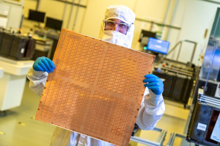
A test glass core substrate demonstrated by Intel
Currently, mainstream AI chips, including NVIDIA GPUs, use substrates mainly made of ABF materials. The biggest drawback is that they are prone to bending and deformation when heated. A one - meter - long ABF carrier board will expand by about 15 microns for every 1°C increase in temperature.
In contrast, the silicon chips placed on top of the ABF carrier board hardly deform when heated.
Therefore, when the chip generates heat during operation, the bottom ABF substrate expands outward due to heat, while the upper silicon chip remains unchanged, causing the entire substrate to bend, that is, "warpage".
The larger the chip size, the more severe the warpage. Imagine a credit card with all four corners arching up at the same time. The consequences can be catastrophic.
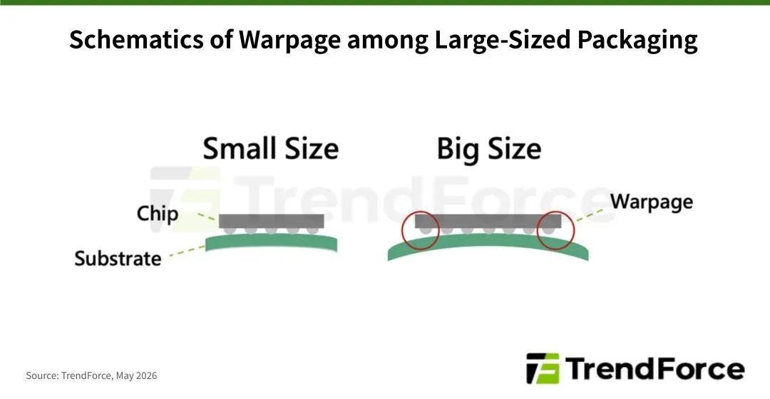
The larger the carrier board size, the more obvious the warpage; Image source: TrendForce
This is why glass substrates have been brought to the table. Since their "heat - resistance" is comparable to that of silicon chips, even if they deform at high temperatures, they can remain synchronized with the silicon chips, effectively avoiding warpage.
Compared with Intel, the carrier board that TSMC wants to replace is at a higher level - the bare die layer of the chip.
A GPU bare die consists of a computing core unit (CPU/GPU) and multiple HBMs, which are placed on a silicon interposer. This silicon interposer is the board that TSMC most wants to replace.
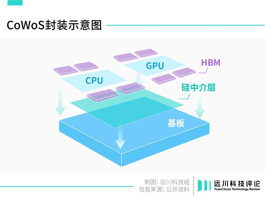
The manufacturing cost of a silicon interposer is extremely high. The unit price of a large - size silicon interposer exceeds $100[2]. In comparison, the single - unit purchase price of the A19 Pro in the iPhone 17 Pro Max is only $90.
Moreover, compared with these mobile phone SoCs with powerful computing capabilities, the main function of a silicon interposer is just data transfer, which is like buying a small electric scooter at the price of a sports car. It sounds even more of a loss.
The size of the silicon interposer is directly related to the size of the AI chip and the number of HBMs used. As AI chips become larger and more HBMs are used, the cost of the silicon interposer is also increasing.
For manufacturers buying AI chips, it's like spending $100,000 on a car and then having to spend another $50,000 on a license plate to drive it on the road.
The biggest advantage of using a glass substrate to replace the silicon interposer is that it is cheap. For the same size, the cost is less than half of the latter[2].
The ideas of Intel and TSMC are reasonable, but the implementation of new technologies has never been an easy task. Especially in the chip industry, new technologies not only challenge the laws of physics.
Chip manufacturing is the most complex activity humans have ever engaged in. Over the past half - century, a set of extremely strict rules has been established, and the upstream and downstream industries have closely constructed a standard system. A small adjustment can have a far - reaching impact.
Even the slightest adjustment may involve the adjustment or even a complete overhaul of upstream equipment and materials.
So, while the giants talk boldly about innovation, they act conservatively and cautiously.
Intel proposed the concept of a glass core carrier board in 2023, and the mass - production time is only vaguely set between 2026 and 2030. TSMC has been very secretive about its CoPoS plan. Only recently did it publicly reveal for the first time that it will take 2 - 3 years to reach a certain scale.
However, several major forces have forcefully advanced the progress.
Who is Pushing the Progress
The first major force is NVIDIA.
Just a few months after Intel officially announced the glass core substrate, Morgan Stanley released a report predicting that the GB200 "might" be packaged using a glass substrate.
This report was once over - interpreted as "NVIDIA officially announcing that the GB200 will use a glass substrate", and related concept stocks soared again in the chaos.
Putting aside the misunderstanding, the fact that a speculation without any official endorsement can be so convincing is also because in the public's perception, NVIDIA indeed has the greatest motivation to promote the implementation of glass substrates.
NVIDIA's GPUs account for 9 out of 10 AI computing power chips. With the exponentially increasing demand for computing power, each generation of GPUs is trying to stack more transistors, resulting in larger and larger GPUs.
The area of the B200 is almost twice that of its previous generation, the H100, and is nearly 10 times that of Apple's M2 Ultra chip. It is about the size of half a bank card, which has reached the warpage limit that an ordinary IC carrier board can bear.
The Rubin, which will be mass - produced in the second half of the year, is even larger than the B200. Replacing the material is not an option but a necessity.
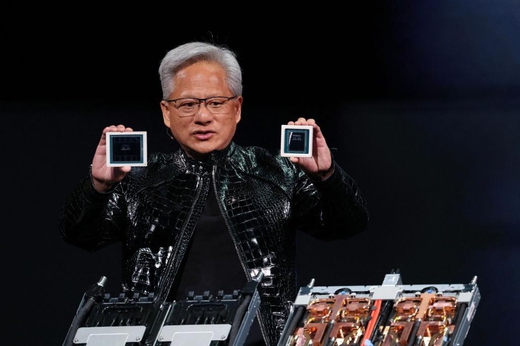
Jensen Huang holds the B200 in his left hand and the H100 in his right hand
In March this year, NVIDIA officially announced a full - scale shift to glass substrates. The Rubin took the lead in the trial, advancing the commercialization node of glass substrates to the end of this year.
With NVIDIA leading the way, there is an unexpected force pushing from behind. It is not from the upstream of the chip industry but from the neighboring industry - the panel industry.
Before being used in chip packaging, the largest downstream application of glass substrates was display panels.
The inside of a display panel has a sandwich structure. The two "slices of bread" are glass substrates, one for controlling brightness and the other for controlling color.
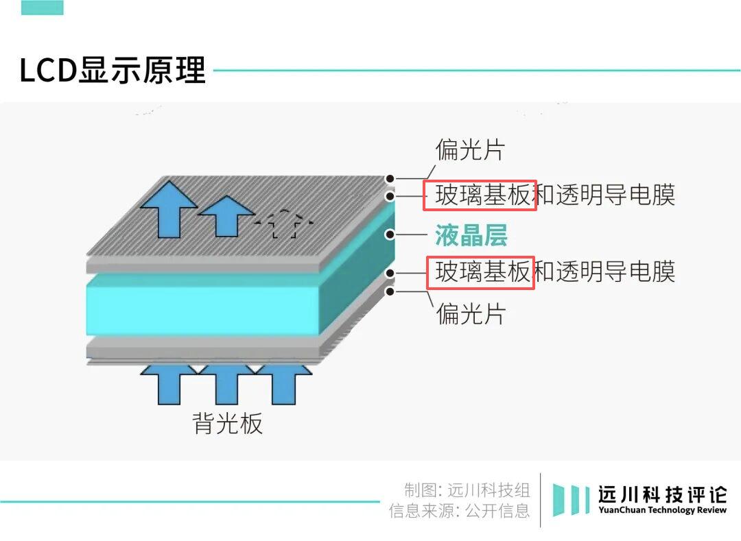
The glass substrate in an LCD panel
The precision processing technology and equipment used in display panels have a very high degree of overlap with the glass substrate technology used in chips. Exaggeratingly speaking, high - end production lines can be modified for use.
Therefore, in the implementation of glass substrates, the most active players are actually from the panel industry.
For example, Innolux, a major panel manufacturer in Taiwan, China, planned to transform into chip packaging as early as 2019.
During the fierce global panel price war, Innolux was struggling. It accepted an offer from the Industrial Technology Research Institute of Taiwan, jointly developed chip packaging technology based on glass substrates, and started to transform its panel production lines.
By 2023, when Intel officially announced the glass substrate technology, Innolux had built the world's first FOPLP packaging production line transformed from a panel production line.
The following year, it won large orders from chip giants NXP and STMicroelectronics. It also sold an idle 5.5 - generation panel line to TSMC at a high price to relieve the latter's shortage of advanced packaging capacity.
At the beginning of this year, the monthly output of Innolux's FOPLP advanced packaging production line had increased tenfold to tens of millions. It not only firmly held on to TSMC but is also rumored to have entered the supply chain of SpaceX's Starlink.
The panel manufacturers in Taiwan, China are working hard, and their counterparts on the Chinese mainland are also making rapid progress.
BOE started researching and developing glass substrates in 2020. In 2024, it invested nearly 100 million yuan to build a test line, and in the first half of this year, it achieved full - automation of the equipment line[4].
Currently, it has started sending samples to customers for testing and verification. The cooperation with Corning in May is to secure the supply of upstream special glass in the next few years, and large - scale mass production is imminent.
The Chinese mainland controls more than 60% of the world's panel production capacity. Especially for high - generation panels, it has the most mature and highly automated production lines. The greater advantage lies in the complete upstream industrial chain for cooperation.
Currently, several companies that the secondary market is most concerned about, such as Dier Laser, Han's Laser, and Delong Laser, are at the most upstream, manufacturing TGV (Through - Glass Vias) laser micro - hole equipment. Vog Optoelectronics is in the middle, processing glass substrates.
In addition to Chinese manufacturers, South Korea's Samsung Electro - Mechanics, LG Innotek, Japan's Dai Nippon Printing, and Nippon Electric Glass are all active in the field of glass substrates. They are also familiar faces that have emerged from the panel war.
With financial support for demand and assistance from the neighboring industry, glass substrates have quickly progressed from being severely criticized as "concept hype" to the "eve of mass production". Brokerage institutions have changed their cautious attitude and are painting a bigger picture.
Objectively speaking, there are still several technical challenges to overcome before the large - scale implementation of glass substrates.
For example, in terms of the core material, special glass, currently only Corning can process up to 11 layers without breakage, while the domestic supply chain can only achieve 3 - 4 layers at most[5]. Another example is the insufficient process of copper electroplating equipment[5].
According to industry chain estimates, the large - scale production of glass substrates will not happen until the end of 2027 at the earliest.
The end of computing power is electricity, but before reaching this end, the industry chain may have to cross one more hurdle - glass substrates.
References
[1] Research on the warpage of 2.5D CoWoS packaging based on glass substrates, Shi Hangbo, Wang Xu, Fan Jilei, etc.
[2] The unit price of large - size silicon interposers exceeds $100, accounting for half of the cost. How can AI computing power chips break through the bottleneck of packaging costs? Yue Investment Advisor
[3] A complete breakdown of TGV glass perforation: After Intel's glass substrate appears, understand the hard thresholds, the countdown to mass production in 2027, and the investment map of the Taiwan supply chain, Sinopac Securities
[4] BOE: The test line for glass - based packaging carrier boards has been connected, with a designed production capacity of 1,000 pieces per month. Future Semiconductor
[5] Industry exchange on glass substrates, Summary Research Report
This article is from the WeChat official account "Yuanchuan Technology Review" (ID: kechuangych). Author: He Luheng, Editor: Li Motian. Republished by 36Kr with permission.