What's the progress of the industrialization of glass substrates?
At the CSPTxITG V2026 conference on glass substrates, a set of exciting data emerged: As the core material for next-generation advanced packaging, glass substrates are entering an accelerated period of industrialization. The global market size is expected to grow rapidly from $1.48 billion in 2024 to $2.33 billion in 2034. The technological competition is becoming increasingly fierce, and companies such as Intel, Samsung, and the JOINT3 Alliance are accelerating their layouts.
However, despite the excitement, frontline practitioners remain sober and restrained. In conversations with companies in the industrial chain, we heard a different version of the story: The mainstream process route has only recently converged on "femtosecond laser induction + wet etching." The consistency issue of copper electroplating filling has not been completely resolved, and a complete industry standard system is still lacking. A industry expert even stated bluntly that the industrial application of glass substrates will not occur until at least after 2030.
The application and implementation of glass substrates is a long-distance race involving equipment, materials, processes, standards, and patience.
01
Why Must It Be Glass?
Why have glass substrates been included in the next-generation high-performance packaging roadmaps of NVIDIA, AMD, and Intel?
This is mainly due to the physical properties of glass:
First, extremely low dielectric loss. The Df value of glass substrates is as low as 0.001 - 0.003 (@10GHz), which is 10 times lower than that of traditional FR-4 organic substrates. It can support high-speed signal transmission exceeding 112Gbps. In the interconnection scenarios of 112Gbps/PAM4 and even the next-generation 224Gbps, this is a physical limit that organic materials cannot reach.
Second, excellent CTE matching with silicon wafers. The coefficient of thermal expansion (CTE) of glass is 3.0 - 8.0×10⁻⁶/K, which is highly compatible with silicon chips (2.6×10⁻⁶/K). This fundamentally eliminates the solder joint fatigue and delamination failure caused by thermal cycling, which is a prerequisite for the long-term stable operation of high-end AI chips under a power consumption of several kilowatts.
Third, ultra-high surface flatness. The surface roughness of glass is less than 0.1μm, which is 1/50 of that of organic substrates. It can ensure the high-precision etching of fine circuits (<5μm L/S) and the alignment accuracy of massive transfer.
Fourth, high thermal conductivity and heat resistance. The thermal conductivity of glass is 1.1 - 1.4 W/m·K, and the operating temperature is >500°C. It can perfectly meet the heat dissipation requirements of high-power chips, and its Tg value far exceeds the upper limit of organic materials. When the power consumption and area of AI chips reach their limits, glass substrates are the only material that can provide an increase at the physical level.
Internationally, Intel positions itself as a "technology integrator + ecosystem builder," focusing on the packaging of CPUs, silicon photonics modules, and AI chips. It collaborates with Corning, Schott, and Asahi Glass to promote ecosystem construction and plans to achieve large-scale application between 2026 and 2030. It also reaffirmed the strategic position of glass substrates at IMAPS 2025. Samsung Electro-Mechanics has a joint venture with Sumitomo Chemical to produce glass cores. The pilot production line at its Sejong factory has achieved a TGV aspect ratio of 10:1. It not only supplies samples of the "Baltra" AI server chips to Apple but also promotes Samsung Electronics to test glass substrates for HBM4 packaging. At the same time, it invests in Extol to strengthen the supply chain for metal surface treatment. SKC/Absolics, as a "pioneer in mass production," has built the world's first mass production-level factory in Georgia, USA. It has provided mass production-level samples to AMD for certification and plans to start small-scale mass production in 2026. It has achieved a process breakthrough with a void ratio of <0.5% in copper filling. TSMC adopts a relatively cautious follow-up strategy. It is building its first CoPoS pilot production line in Chiayi, Tainan. It plans to establish the production line in 2026, initially using the 300mm specification. It also cooperates with Corning to develop special glass carriers. The packaging area roadmap plans to achieve 5.5 times the reticle size in 2026 and expand to 14 times between 2028 and 2029.
From the perspective of the competitive landscape, three major camps have emerged globally. The US camp, represented by Intel, Absolics, and Corning, follows a vertically integrated route of "independent R & D + government funding." It takes advantage of the policy dividends of the CHIPS Act and the customer resources of Intel/AMD to gain a technological first-mover advantage, with a cumulative investment of nearly $2 billion. The Korean camp consists of Samsung Electro-Mechanics, LG Innotek, and SKC, forming a "electronics + display + materials" group synergy army. Relying on the internal synergy within the Samsung Alliance for rapid iteration and the strategy of binding with major customers, the total investment reaches $1.15 billion. The Japanese camp is linked by the JOINT3 Alliance, which unites established material giants such as AGC, DNP, and Schott. Through the "alliance co-creation" model, it builds an entire industrial chain ecosystem. Relying on its profound material technology accumulation and traditions in precision manufacturing, it makes steady progress.
02
The Stealth Battle of TGV: Hole Drilling and Filling
The core process of glass substrates is TGV (Through Glass Via). However, according to frontline equipment manufacturers, the industrialization of TGV is far from simple.
Hole Drilling: The Process Route Has Just Converged
Equipment manufacturers restored the technological evolution of TGV hole drilling for us: "The industry has previously explored various routes such as sandblasting, mechanical drilling, laser ablation, and pure chemical methods, but none of them could meet the requirements. It was not until the combination of femtosecond laser induction and wet etching that it became the most stable mainstream solution at present."
The principle is as follows: The instantaneous power of the femtosecond laser is extremely high, which produces a nonlinear optical effect on the glass substrate and induces a modified area. Then, the substrate is immersed in a chemical solution, and the induced area is preferentially corroded to form a through-hole. By controlling the circulation of the chemical solution, the taper of the hole can be optimized from 50% to nearly 100% (completely vertical), while avoiding the microcracks and rough sidewalls caused by conventional drilling. The roughness of the sidewalls directly affects the adhesion of the subsequent PVD seed layer and electroplated copper. If the hole wall is too rough, the copper layer is likely to fall off, ultimately leading to conductive failure or glass breakage.
Han's Laser, the leading domestic manufacturer of wafer-level TGV equipment, mentioned: "Most of the domestic equipment for wafer-level TGV uses our products. The main competitors try to win orders with low prices." According to its introduction, there are about 6 - 8 domestic equipment manufacturers focusing on TGV hole drilling. In addition to Han's Laser, the equipment of Guihua Intelligence has also been recognized by customers such as BOE.
Hole Filling: The Real 'Hard Nut to Crack'
However, hole drilling is only the first step. The real bottleneck in the industry lies in copper electroplating filling.
A practitioner stated bluntly: "Hole drilling is relatively simple, and electroplating is the most difficult part. Glass substrates have many holes, which are narrow and dense. It is necessary to ensure the consistency of copper filling in each hole and avoid the formation of cavities. Once there are cavities, not only will the conductivity fail, but the glass may also break under thermal stress." Another industry insider further pointed out that the biggest bottleneck in TGV is yield control, including problems such as microcracks and poor filling. Some of these problems will only be exposed in reliability applications. He suggested that the industry should first implement wafer-level business, stabilize the yield and reliability through the traction and verification of specific products, and then develop towards panel-level to reduce costs and improve efficiency.
A CMP equipment practitioner said that the core problems are concentrated in two dimensions: electroplating uniformity and hole filling degree. He said that during the sample-making process some time ago, there were frequent cases of unfilled holes. This quality defect will cause a serious chain reaction: not only will it directly lead to conductive failure and glass breakage under thermal stress, but it will also make downstream enterprises reluctant to purchase subsequent CMP (Chemical Mechanical Polishing) equipment rashly. Once the yield in the electroplating process cannot be guaranteed, the investment in expensive CMP equipment will face a huge risk of idleness.
Currently, domestic enterprises that started glass substrate processing earlier include BOE, Vog Optoelectronics (Tongge Micro), Xiamen Yuntian, Fozhixin, Triassic (Maike), Anjielemeike, and Chengdu Yicheng. However, these enterprises generally purchase very few CMP equipment. The fundamental reason is that the bottleneck in the electroplating process has not been broken through. In order to meet the requirements of sample-making and small-scale production of high-precision products, many enterprises can only choose to send their samples to South Korea for processing. However, this solution is extremely costly and faces serious transportation problems: glass substrates are large in size, thin, and brittle, and are very likely to break during transportation. Enterprises dare not send them by express delivery and can only adopt methods such as customer self-pickup, special vehicle escort, or even manual carrying, which greatly increases the time and economic costs.
This means that although the "10:1 aspect ratio" of TGV has been achieved in the laboratory, there are still three major mountains between the laboratory and the production line: yield, reliability, and consistency.
03
Equipment and Materials: The 'Chokepoints' Hidden Deep in the Industrial Chain
In the glass substrate industrial chain, the investment in a single production line for equipment exceeds $100 million. However, behind the huge investment, many segments still rely on imports or are not yet mature.
Non-Contact Handling of Ultra-Thin Glass
In the processing of glass substrates, a very important but easily overlooked link is handling.
Suzhou Xinjunzheng distributes Bernoulli wafer fingers imported from Japan, which are specifically used for non-contact handling of glass substrates. The principle is to use the Bernoulli effect of "high flow velocity, low air pressure" to "lift" the product through air pressure and strictly control the pressure within 0.35 MPa with the cooperation of solenoid valves and pressure gauges.
"Glass substrates are very brittle and extremely thin, and the current thickness can reach 0.1 millimeters," the supplier introduced. "Vacuum adsorption is likely to leave hard marks, while Bernoulli wafer fingers are non-contact and will not damage the product. However, the cost of Bernoulli wafer fingers is much higher than that of products based on the vacuum adsorption principle. The equipment is expensive and difficult to manufacture. The client will calculate the return on investment and value the product efficiency and breakage rate."
Currently, the handling equipment for ultra-thin glass substrates below 200 microns is mainly imported from Japan. However, downstream customers have now required production in China. The Japanese side provides the drawings and systems, and Chinese suppliers can supply products only after being approved by the Japanese side to ensure the ultimate stability of "being problem-free for 5 or 10 years."
This detail reflects the overall dilemma of the glass substrate industry: The semiconductor industry may not have extremely high requirements for performance, but it has extremely strict requirements for stability. Any small fluctuation in any link will be exponentially magnified in the subsequent processes.
Laser and Electroplating: The Two Poles of Domestic Substitution
In the TGV laser drilling process, domestic equipment has certain competitiveness. Han's Laser occupies the leading position in domestic wafer-level TGV equipment, and Guihua Intelligence has been recognized in the field of laser-assisted hybrid etching. Enterprises such as Dier Laser have also made in-depth layouts in the femtosecond laser induction process. However, in the processes of PVD coating, electroplating equipment, and testing equipment, relying on imports is still a reality. In particular, the electroplating copper filling equipment directly determines the upper limit of the TGV yield, and the equipment capabilities of domestic enterprises in this process are significantly weaker than those in laser drilling.
The same is true on the material side. High-purity TGV glass substrates currently mainly rely on Japanese and American enterprises such as Schott, Corning, and Asahi Glass. Although domestic enterprises such as Rainbow Co., Ltd. have made certain progress in the field of TGV glass substrates, the overall product strength is still inferior to that of foreign brands. Many domestic glasses are prone to breakage problems during processing such as laser drilling and wet etching, resulting in a significant decrease in yield. At present, large-scale substitution has not been achieved. The core patents for domestic glass formulations and drilling processes are still monopolized by overseas companies.
04
Lack of Standards and Pilot Test Platforms
If technology and equipment are the "hard constraints," then the "soft environment" of the industrial ecosystem is the key to determining whether glass substrates can transition from "samples" to "commodities." The lack of mature experience for reference is the top pain point of the current glass substrate industry: uncertain technology routes, lack of a standard system, and difficulty in yield improvement. A downstream customer suggested: "The industry should formulate unified substrate specifications, covering basic indicators such as warpage and aspect ratio. If the standards are not universal, the design, manufacturing, and packaging and testing ends will operate independently and make repeated mistakes."
Another frequently mentioned keyword is "pilot test platform." Some experts suggested: "Build a public platform and establish a pilot test line to allow small and medium-sized enterprises to make mistakes at low cost and accelerate technological iteration." Moreover, currently, some domestic AI design companies have started testing large computing power chips based on glass substrates, but the early binding mechanism of "joint optimization from the chip definition stage" has not been established. Most projects still remain in the passive mode of "modification after tape-out," which greatly prolongs the verification cycle.
A practitioner even stated bluntly: "Although there is supply chain capability in China, there is a lack of an outlet. It is recommended to cooperate with Huawei to form a concept of competition and cooperation." Another university expert also said that universities and research institutions can formulate an innovation chain roadmap from the top-level architecture, and the industrial alliance needs to attract more downstream enterprises to clarify product requirements in order to truly accelerate the industrialization of technology.
Although the packaging of AI/HPC chips is regarded as the "biggest incremental scenario" for glass substrates, almost all interviewees believe that large-scale application has not been achieved, and optical modules and radio frequency are the most realistic breakthrough points at present.
The analysis of Vog Group also supports this judgment: The low dielectric loss characteristics of glass substrates give them significant advantages in 800G/1.6T optical modules, CPO (Co-Packaged Optics), and 5G/6G millimeter-wave radio frequency front-end modules. In the CPO scenario, glass has excellent transparency in the optical communication band (850 - 1550nm) and can be directly used as an optical waveguide carrier, with a power consumption reduction of more than 70% compared with traditional pluggable optics.
"Give priority to the implementation in scenarios such as optical modules, radio frequency, and MEMS to leverage the low-loss advantages of glass substrates, and then expand to higher-order applications," a downstream customer suggested. These scenarios have relatively loose requirements for extreme packaging sizes but extremely high requirements for signal integrity and thermal management, which happen to match the physical advantages of glass substrates.
Currently, the glass substrate industry is at a crossroads. On the one hand, the mass production schedules of Intel, Samsung, and TSMC have been set, and the "industry's first year" in 2026 seems within reach. On the other hand, the low yield of domestic glass substrates, the unresolved problem of copper electroplating filling, the lack of a standard system, and the shortage of pilot test platforms remind the industry that there is a two- to three-year engineering improvement period between "being able to make samples" and "being able to achieve stable mass production." Glass substrates are "reshaping the value distribution of the entire electronic information industrial chain." From EDA design to terminal applications, seven major links form a complete closed-loop, with a total driven market size of more than $200 billion. However, this reshaping will not happen overnight.
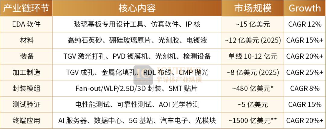
For the domestic industry, the current key task is not to blindly pursue large-scale mass production of panel-level packaging but to improve