Dialogue with HE Tingbo of Huawei: The Real Power and External Misunderstandings of the "Tao (τ) Law"
On May 25th, He Tingbo, the president of Huawei Semiconductor, released the "Tao (τ) Law," which shocked the semiconductor industry and the capital market.
This release responded to the public statement made by Ren Zhengfei, the founder of Huawei, six years ago. In 2020, Huawei was included in the Entity List. Ren Zhengfei, who rarely appeared in public, frequently accepted interviews from Chinese and foreign media that year and mentioned basic research, basic education, mathematics, and physics many times. These topics seemed far from Huawei, which was almost on the verge of supply cut - off at that time.
Facing a huge crisis, a company's instinctive reaction is often to send an immediately visible self - rescue signal to the outside world, such as adjusting the supply chain, seeking policy support, and releasing alternative solutions. These measures are short - term and immediate, which can effectively stabilize the morale within the company and the confidence of the outside world. Ren Zhengfei's repeated emphasis on the proposition of basic research seemed a bit "mysterious and impressive" and "a distant water that can't quench the immediate thirst" at that time.
Looking back six years later, the strategy and tactics have formed a closed - loop.
On May 25th, He Tingbo told us, There are two "ten - year judgments" within Huawei: First, Moore's Law will "hit the wall" within the next ten years. Even without external blockades, the economic and physical limits of advanced processes will become a common constraint for the entire semiconductor industry. Second, in 2020, Huawei internally predicted that it would take ten years to make a breakthrough in the technical path of logic folding.
The actual progress was faster than expected. He Tingbo's team achieved results in six years.
He Tingbo is the president of Huawei's Semiconductor Business Department and the director of Huawei's Scientists Committee. At the end of 2019, in an internal letter to all employees of HiSilicon, she mentioned, "In the future, there won't be another ten years to build a spare tire and then replace it. The buffer zone has disappeared. Every new product must have a'scientific and technological self - reliance' plan from the very beginning."
He Tingbo said that in the past six years, she had moments of frustration. When the path of advanced processes was blocked by external forces, and Moore's Law itself was hitting both economic and physical walls globally, the research direction was once pushed into a dead end.
How to achieve inter - generational performance improvement when it is difficult to make breakthroughs in semiconductor process technology? The turning point came from a water conservancy project more than 2000 years ago - Dujiangyan. At the most difficult time, He Tingbo took her team to Dujiangyan to relax.
Without electricity, Turing mechanics, or modern machinery, the ancients, relying only on their insights into "mountains, water, and trends," achieved automatic flow diversion, sediment discharge, and flow control through dam - less water diversion. She suddenly realized that when external constraints cannot be changed, the key to solving the problem lies not in waiting for the conditions to improve, but in "re - examining these (available) conditions to solve the problem."
"Even without export controls, Moore's Law will become a constraint for everyone in the next ten years. Huawei is just working under this constraint earlier." He Tingbo repeatedly emphasized a deeper industrial reality: After the chip process reached 7nm (nanometers), the design cost and wafer cost of each generation of process have increased exponentially, and the speed of the decline in unit transistor cost has slowed down irreversibly. The economic universality of advanced processes is coming to an end. In other words, the global semiconductor industry is already at the door of a paradigm shift. Huawei was just pushed over the threshold earlier due to the blockade.
The superposition effect of "the inevitability of the industry" and "Huawei's urgency" constitutes the dual background for the birth of the Tao Law.
In fact, it is more like a general problem - solving framework for the post - Moore era. This framework was first put forward by a Chinese company that was cut off from supplies, and its feasibility has been verified with 381 mass - produced chips. During the communication after the speech, He Tingbo emphasized: "If we could still obtain the most advanced EUV lithography machine today, would we still take this path? The answer is not necessarily. But history doesn't have 'what - ifs'. It was precisely the loss of the right to choose that made us hit the problem that all players will eventually face ten years earlier."
01
The inevitability of the industry, Huawei's urgency
Even without the blockade, Moore's Law will hit the wall within ten years. Huawei just lost the right to choose earlier.
In He Tingbo's view, after 7nm, the economic foundation of semiconductor advanced processes is changing.
In the past 40 years, the reason why Moore's Law has been able to continuously drive the development of the entire semiconductor industry is not only because the number of transistors has been continuously increasing. More importantly, the speed of the increase in transistor density has been faster than the speed of the increase in manufacturing cost for a long time. This means that although the chip manufacturing cost will increase, the unit transistor cost is still decreasing continuously. The cost dividends released by technological progress can be shared by the entire industrial chain and consumers.
"The biggest advantage of Moore's Law in the past was that it could continuously share the dividends brought by technological progress with the entire industrial community. But today, it is becoming more and more difficult for advanced processes to continue to release such dividends." He Tingbo said.
She believes that in this situation, continuing to rely on geometric shrinkage to improve performance will inevitably lead to a path of "continuous cost increase." In contrast, the τ (Tao) Law does not simply rely on more expensive advanced transistors. Instead, it uses the technical means of logic folding to increase transistor density, optimize the delay and performance of devices, circuits, chips, and systems, and thus achieve the continuous evolution of semiconductor and electronic systems.
The economic benefits brought by Moore's Law have been gradually slowing down in the past three years. This is also a recognized problem in the current semiconductor industry. There has been a large amount of academic research in the semiconductor industry in the past five years.
The international top - level academic journal Science published a paper in its June 2020 issue, co - authored by Charles E. Leiserson, a professor at the Massachusetts Institute of Technology and a Turing Award winner, and researchers from NVIDIA, Microsoft, etc. - There’s Plenty of Room at the Top: What Will Drive Computer Performance after Moore’s Law?
The core idea of this paper is that in the "post - Moore era," the improvement of computing performance will increasingly rely on the collaborative optimization of software, algorithms, system architectures, and dedicated hardware, rather than mainly relying on the continuous reduction of transistor size.
Similar to the above view, Huawei's internal judgment is that Moore's Law will "hit the wall" after ten years.
Although advanced processes can still continuously improve transistor density, performance, and energy efficiency, the design cost, manufacturing cost, and capital expenditure required for each generation of process nodes are rising rapidly. Especially after the semiconductor process entered the 5nm, 3nm, and even 2nm stages, the cost of advanced processes has increased significantly.
Data from the international semiconductor consulting firm IBS (International Business Strategies) in 2022 shows that the design cost of a 7nm chip is about $249 million, a 5nm chip is about $449 million, a 3nm chip is about $581 million, and a 2nm chip is about $725 million.
Research by the Center for Security and Emerging Technology (CSET), an international semiconductor think - tank, shows that the cost of a 300mm wafer for TSMC's 7nm process is about $9,346, and for the 5nm process is about $16,988. Data from the international semiconductor market research firm TrendForce shows that the price of a 3nm wafer has reached about $25,000 - $27,000, and for a 2nm wafer it is about $30,000.
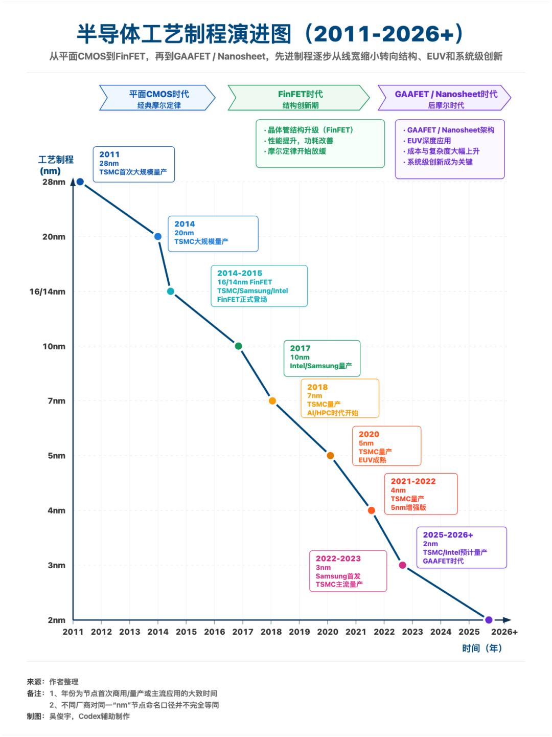
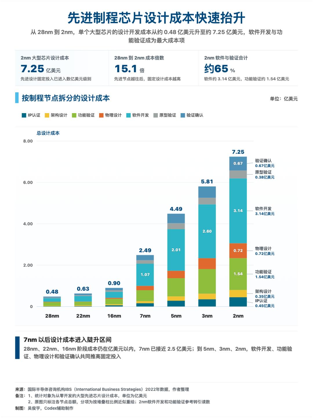
The industry - wide inclusive effect of Moore's Law, where performance improvement and unit cost reduction occur simultaneously, is irreversibly weakening. After entering the era of advanced processes, only a few leading wafer foundries and a few technology companies such as Apple and NVIDIA, which can bear the R & D and mass - production costs of next - generation chips, can still continuously enjoy the performance and energy - efficiency dividends brought by advanced processes.
For Huawei, this happened earlier. After being included in the "Entity List" in 2019, Huawei was forced to start looking for another route - no longer just pursuing an increase in the number of transistors per unit area, but continuing to improve performance by reducing the "time cost" in the system. Against this background, the Tao (τ) Law was born.
It is a theoretical fact that needs to be clarified that the concept of Tao (τ, also known as the time constant) was not first proposed by Huawei.
In the fields of electronics and semiconductors, τ has long been used to describe the time delay in circuits and the influence of RC (resistance, capacitance) characteristics on the signal propagation speed. In the past few decades, the semiconductor industry has accumulated a large amount of research around reducing time delay, including directions such as interconnection optimization, timing optimization, advanced packaging, short - distance communication, asynchronous computing, and data - flow architecture. Their common goal is to reduce the propagation time cost of information in devices, circuits, chips, and systems.
Many chip engineers told us their views on the Tao (τ) Law. They mentioned that the optimization idea centered on reducing time delay is not a new concept in the industry. Previously, technologies such as the 3D stacking of HBM (High - Bandwidth Memory) and the Hybrid Bonding advocated by AMD have practiced this direction to varying degrees.
A chip engineer mentioned that the 3D technology of HBM, which stacks multiple DRAM (Dynamic Random - Access Memory) chips vertically in an overlapping package, and the Hybird Bonding (a technology that uses direct copper - to - copper metal connection and dielectric materials such as silicon dioxide) advocated by AMD, both adopt a similar idea.
However, during the period when Moore's Law was long - term effective, these technologies were more regarded as auxiliary optimizations for the reduction of process technology and were not the core main line of industrial evolution. The uniqueness of Huawei lies in being the first to propose that the "Tao (τ) Law" should be the main direction of evolution.
After being included in the Entity List in 2019, facing a complete supply cut - off, Huawei had to try another route - no longer just pursuing an increase in the number of transistors per unit area, but continuing to improve performance by reducing the "time cost" in the system.
The Tao (τ) Law starts with chips but is not limited to chips. He Tingbo especially emphasizes the "Cost Effective" brought by the Tao (τ) Law. It does not rely on advanced processes such as EUV. Instead, it reduces the dependence on high - cost manufacturing tools through the optimization of time constants at various levels such as devices, circuits, chips, and systems.
Its complete idea is to take "reducing τ" as a unified optimization goal from all aspects such as transistors, circuits, chips, and systems. Specifically, it reduces the switching delay at the transistor layer, reduces the RC propagation delay at the circuit layer, reduces the calculation and access delay at the chip layer, and reduces the synchronization and communication delay at the system layer.
Therefore, the Tao (τ) Law is also applied in a larger computing system, including super - nodes and even computing power clusters.
Computing starts with the current and data transmission of transistors in a chip. Hundreds of billions of transistors are etched on a single chip, and they control the signal switches. A chip is then connected to devices such as HBM through packaging technology. Dozens of chips are deployed in a server cabinet, multiple cabinets form a super - node, and hundreds or thousands of super - nodes are further connected to form a large - scale computing power cluster. From the signal transmission of transistors to the efficient throughput of Tokens (tokens) in the computing power cluster, the entire process is essentially about shortening the transmission time of data and information.
Computing power is no longer just improved through a single chip. It requires a systematic project to be comprehensively improved.
02
Why the Kirin chips?
The unit area and power consumption budget of mobile phone chips are extremely limited. The physical constraints make the design of mobile phone SoCs much more difficult than that of AI computing power chips. If the Kirin chips can achieve this, it will be the best verification.
The Kirin series of chips installed in Huawei mobile phones are among the first chips to be transformed using logic folding. The Kirin 2026, which will be installed in Huawei's flagship mobile phones in the second half of 2026, is a chip transformed based on the Tao (τ) Law and has already been mass - produced.
According to the information disclosed by Huawei, the transistor density of the Kirin 2026 has increased by 53%, and the main frequency has increased by nearly 13%.
He Tingbo's signed paper A Time Scaling Theory for Multi - Layer Electronic Systems published on the pre - release platform of scientific papers of the Chinese Academy of Sciences shows that the performance improvement of the Kirin 2026 used to take "three years of geometric shrinkage" to achieve.
In this paper, He Tingbo presented the roadmap for the Kirin series of chips in the next few years. The core frequency of the Kirin CPU is shifting from a small increase relying on the planar architecture in the past to a three - dimensional integration route relying on LogicFolding.
From 2023 to 2025, the main frequencies of the Kirin 9000s, Kirin 9020, and Kirin 9030 Pro are 2.6GHz, 2.65GHz, and 2.75GHz respectively. But starting from 2026, the main frequency of the Kirin chips using logic folding technology is expected to increase to 3.1GHz and further reach 4GHz in 2029.
Huawei has not officially disclosed the corresponding process technologies for these chips in the future.
However, relevant Huawei personnel told us that without simply relying on traditional geometric shrinkage, the performance and energy - efficiency ratio of the Kirin chips are still improving. But directly comparing with traditional process technologies does not conform to the development path of the Tao (τ) Law. "Reducing τ" is the key to subsequent evolution.
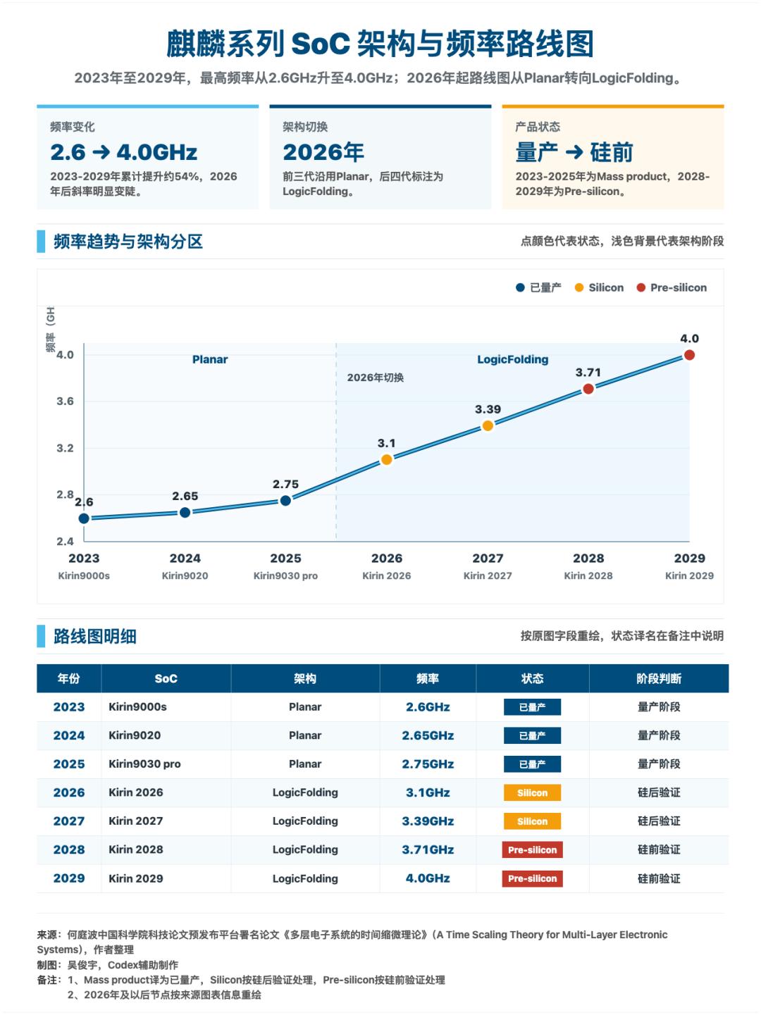
According to He Tingbo, the key technology for "reducing τ" is logic folding.
Logic folding refers to re - dividing the logic circuit that was originally spread out on a single die and conducting high - density logic design on two upper and lower dies. It requires the key path, clock tree, and data bus to participate in the re - design together, so that the two layers together form a unified logic system.
The core goal of this approach is to shorten the signal propagation time, rather than just increasing the packaging density. It is more like folding a logic system into a three - dimensional structure, rather than simply stacking or connecting two chips.
He Tingbo believes that a common misunderstanding is to confuse logic folding with 2.5D/3D packaging or other technologies. In her view, Folding is not the same as Stacking. Stacking is more like the packaging connection of multiple modules, while folding is more like re - designing a originally planar logic system in three - dimensional space.